AO3419L MOSFET Equivalente. Reemplazo. Hoja de especificaciones. Principales características
Número de Parte: AO3419L
Tipo de FET: MOSFET
Polaridad de transistor: P
ESPECIFICACIONES MÁXIMAS
Pdⓘ - Máxima disipación de potencia: 1.4 W
|Vds|ⓘ - Voltaje máximo drenador-fuente: 20 V
|Vgs|ⓘ - Voltaje máximo fuente-puerta: 12 V
|Id|ⓘ - Corriente continua de drenaje: 3.5 A
Tjⓘ - Temperatura máxima de unión: 150 °C
CARACTERÍSTICAS ELÉCTRICAS
trⓘ - Tiempo de subida: 6.7 nS
Cossⓘ - Capacitancia de salida: 77 pF
RDSonⓘ - Resistencia estado encendido drenaje a fuente: 0.075 Ohm
Encapsulados: SOT23
Búsqueda de reemplazo de AO3419L MOSFET
- Selecciónⓘ de transistores por parámetros
AO3419L datasheet
ao3419l.pdf
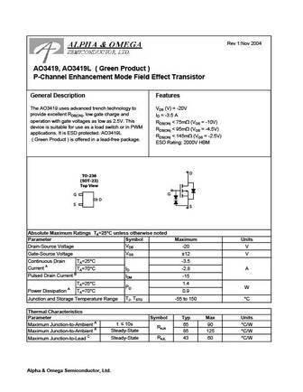
Rev 1 Nov 2004 AO3419, AO3419L ( Green Product ) P-Channel Enhancement Mode Field Effect Transistor General Description Features The AO3419 uses advanced trench technology to VDS (V) = -20V provide excellent RDS(ON), low gate charge and ID = -3.5 A operation with gate voltages as low as 2.5V. This RDS(ON)
ao3419.pdf
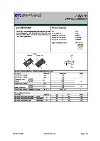
AO3419 20V P-Channel MOSFET General Description Product Summary VDS -20V The AO3419 uses advanced trench technology to provide excellent RDS(ON), low gate charge and operation with gate ID (at VGS=-10V) -3.5A voltages as low as 2.5V. This device is suitable for use as RDS(ON) (at VGS= -10V)
ao3419-3.pdf
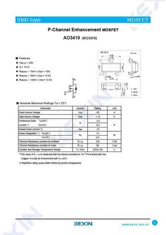
SMD Type IC SMD Type MOSFET P-Channel Enhancement MOSFET AO3419 (KO3419) SOT-23-3 Unit mm +0.2 2.9-0.1 +0.1 0.4 -0.1 Features 3 VDS (V) = -20V ID = -3.5 A RDS(ON) 75m (VGS = -10V) 1 2 +0.02 RDS(ON) 95m (VGS = -4.5V) +0.1 0.15 -0.02 0.95 -0.1 1.9+0.1 -0.2 D RDS(ON) 145m (VGS = -2.5V) 1. Gate 2. Source G 3. Drain S Absolute Maximum Ratings Ta = 25 Parameter Symbol R
ao3419.pdf
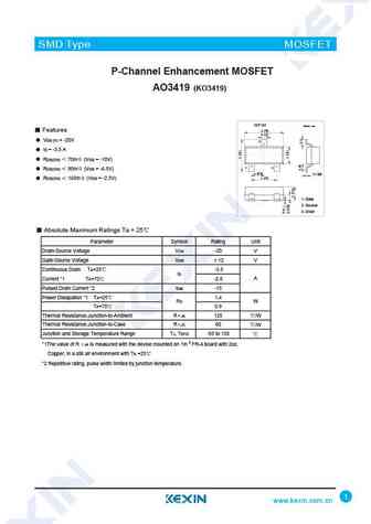
SMD Type IC SMD Type MOSFET P-Channel Enhancement MOSFET AO3419 (KO3419) SOT-23 Unit mm +0.1 2.9 -0.1 Features +0.1 0.4 -0.1 VDS (V) = -20V 3 ID = -3.5 A RDS(ON) 75m (VGS = -10V) 1 2 RDS(ON) 95m (VGS = -4.5V) +0.1 +0.05 0.95 -0.1 0.1 -0.01 +0.1 1.9 -0.1 RDS(ON) 145m (VGS = -2.5V) 1.Base 1. Gate 2.Emitter 2. Source 3. Drain 3.collector Absolute Maximum Ratings Ta =
Otros transistores... 7N80L-TF1-T , 7N80L-TQ2-R , 7N80L-TQ2-T , 7N80G-TA3-T , 7N80G-TF3-T , 7N80G-TF1-T , 7N80G-TQ2-R , 7N80G-TQ2-T , 5N65 , CMP100N04 , CMB100N04 , CMI100N04 , HY4306W , HY4306A , MDF1723 , ME4410AD , ME4970 .
History: DMN67D8L | STD2NB60T4 | 3N70G-TM3-T | WMM08N70C4 | AP4525GEM-HF | RRR040P03TL | BFW10
History: DMN67D8L | STD2NB60T4 | 3N70G-TM3-T | WMM08N70C4 | AP4525GEM-HF | RRR040P03TL | BFW10
🌐 : EN ES РУ

Liste
Recientemente añadidas las descripciónes de los transistores:
MOSFET: ASU70R600E | ASU65R850E | ASU65R550E | ASU65R350E | ASR65R120EFD | ASR65R046EFD | ASQ65R046EFD | ASM65R280E | ASM60R330E | ASE70R950E | ASD80R750E | ASD70R950E | ASD70R600E | ASD70R380E | ASD65R850E | ASD65R550E
Popular searches
2n3569 | 2sd667 | 2sc1111 | bc239 transistor equivalent | 3sk41 | 2sc2240 transistor | c3198 | 2sc793