IPI110N20N3 MOSFET Equivalente. Reemplazo. Hoja de especificaciones. Principales características
Número de Parte: IPI110N20N3
Tipo de FET: MOSFET
Polaridad de transistor: N
ESPECIFICACIONES MÁXIMAS
Pdⓘ - Máxima disipación de potencia: 300 W
|Vds|ⓘ - Voltaje máximo drenador-fuente: 200 V
|Vgs|ⓘ - Voltaje máximo fuente-puerta: 20 V
|Id|ⓘ - Corriente continua de drenaje: 88 A
Tjⓘ - Temperatura máxima de unión: 175 °C
CARACTERÍSTICAS ELÉCTRICAS
trⓘ - Tiempo de subida: 26 nS
Cossⓘ - Capacitancia de salida: 401 pF
RDSonⓘ - Resistencia estado encendido drenaje a fuente: 0.011 Ohm
Encapsulados: TO-262
Búsqueda de reemplazo de IPI110N20N3 MOSFET
- Selecciónⓘ de transistores por parámetros
IPI110N20N3 datasheet
ipi110n20n3.pdf
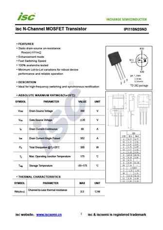
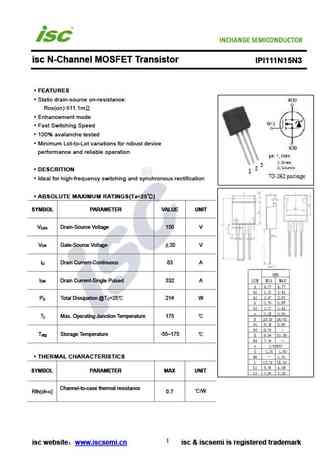
isc N-Channel MOSFET Transistor IPI110N20N3 FEATURES Static drain-source on-resistance RDS(on) 11m Enhancement mode Fast Switching Speed 100% avalanche tested Minimum Lot-to-Lot variations for robust device performance and reliable operation DESCRITION Ideal for high-frequency switching and synchronous rectification ABSOLUTE MAXIMUM RATINGS(T =25 ) a SYMB
ipb107n20n3-g ipp110n20n3-g ipi110n20n3-g ipb107n20n3g ipp110n20n3g ipi110n20n3g.pdf
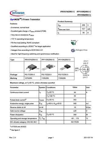
IPB107N20N3 G IPP110N20N3 G IPI110N20N3 G OptiMOSTM3 Power-Transistor Product Summary Features VDS 200 V N-channel, normal level RDS(on),max (TO263) 10.7 mW Excellent gate charge x R product (FOM) DS(on) ID 88 A Very low on-resistance R DS(on) 175 C operating temperature Pb-free lead plating; RoHS compliant Qualified according to JEDEC1) for target appl
ipb108n15n3g ipp111n15n3g ipi111n15n3g.pdf
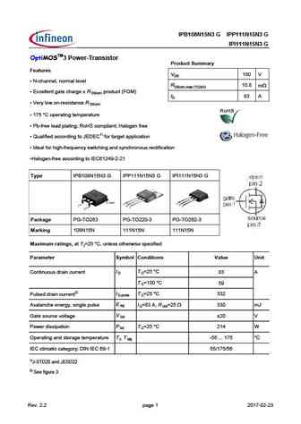
IPB108N15N3 G IPP111N15N3 G IPI111N15N3 G OptiMOSTM3 Power-Transistor Product Summary Features VDS 150 V N-channel, normal level RDS(on),max (TO263) 10.8 mW Excellent gate charge x R product (FOM) DS(on) ID 83 A Very low on-resistance R DS(on) 175 C operating temperature Pb-free lead plating; RoHS compliant; Halogen free Qualified according to JEDE
ipb108n15n3-g ipp111n15n3-g ipi111n15n3-g.pdf
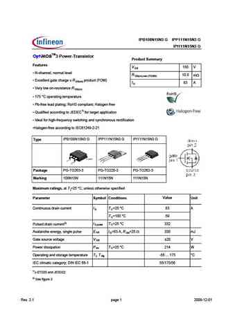
IPB108N15N3 G IPP111N15N3 G IPI111N15N3 G OptiMOSTM3 Power-Transistor Product Summary Features V 150 V DS N-channel, normal level R 10.8 m DS(on),max (TO263) Excellent gate charge x R product (FOM) DS(on) I 83 A D Very low on-resistance R DS(on) 175 C operating temperature Pb-free lead plating; RoHS compliant; Halogen free Qualified according to JE
Otros transistores... IPI041N12N3 , IPI051N15N5 , IPI072N10N3 , IPI075N15N3 , IPI076N12N3 , IPI076N15N5 , IPI086N10N3 , IPI100N08N3 , IRFP260N , IPI111N15N3 , IPI147N12N3 , IPI180N10N3 , IPI200N15N3 , IPI200N25N3 , IPI26CN10N , IPI320N20N3 , IPI35CN10N .
History: ME4174 | NCEP85T14 | PX5S6JZ | GKI10194
History: ME4174 | NCEP85T14 | PX5S6JZ | GKI10194
🌐 : EN ES РУ

Liste
Recientemente añadidas las descripciónes de los transistores:
MOSFET: AUB062N08BG | AUB060N08AG | AUB056N10 | AUB056N08BGL | AUB050N085 | AUB050N055 | AUB045N12 | AUB045N10BT | AUB039N10 | AUB034N10 | AUB033N08BG | AUB026N085 | AUA062N08BG | AUA060N08AG | AUA056N08BGL | AUA039N10
Popular searches
mje15032g datasheet | 2sc2166 | 2sc5198 | 2sc1971 | tip41c transistor datasheet | 2n3907 | 12n60 | mp42b transistor