IPI110N20N3 PDF Specs and Replacement
Type Designator: IPI110N20N3
Type of Transistor: MOSFET
Type of Control Channel: N -Channel
Absolute Maximum Ratings
Pd ⓘ - Maximum Power Dissipation: 300 W
|Vds|ⓘ - Maximum Drain-Source Voltage: 200 V
|Vgs|ⓘ - Maximum Gate-Source Voltage: 20 V
|Id| ⓘ - Maximum Drain Current: 88 A
Tj ⓘ - Maximum Junction Temperature: 175 °C
Electrical Characteristics
tr ⓘ - Rise Time: 26 nS
Cossⓘ - Output Capacitance: 401 pF
Rds ⓘ - Maximum Drain-Source On-State Resistance: 0.011 Ohm
Package: TO-262
IPI110N20N3 substitution
IPI110N20N3 PDF Specs
ipi110n20n3.pdf
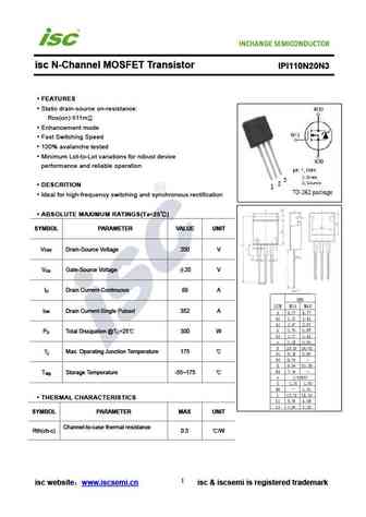
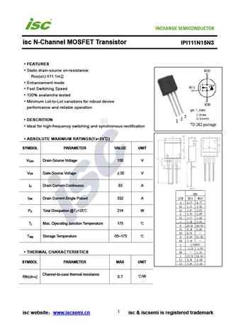
isc N-Channel MOSFET Transistor IPI110N20N3 FEATURES Static drain-source on-resistance RDS(on) 11m Enhancement mode Fast Switching Speed 100% avalanche tested Minimum Lot-to-Lot variations for robust device performance and reliable operation DESCRITION Ideal for high-frequency switching and synchronous rectification ABSOLUTE MAXIMUM RATINGS(T =25 ) a SYMB... See More ⇒
ipb107n20n3-g ipp110n20n3-g ipi110n20n3-g ipb107n20n3g ipp110n20n3g ipi110n20n3g.pdf
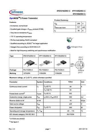
IPB107N20N3 G IPP110N20N3 G IPI110N20N3 G OptiMOSTM3 Power-Transistor Product Summary Features VDS 200 V N-channel, normal level RDS(on),max (TO263) 10.7 mW Excellent gate charge x R product (FOM) DS(on) ID 88 A Very low on-resistance R DS(on) 175 C operating temperature Pb-free lead plating; RoHS compliant Qualified according to JEDEC1) for target appl... See More ⇒
ipb108n15n3g ipp111n15n3g ipi111n15n3g.pdf
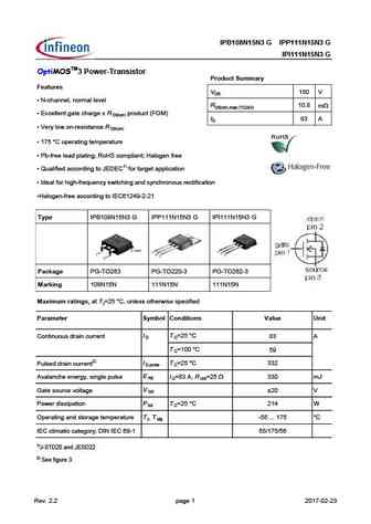
IPB108N15N3 G IPP111N15N3 G IPI111N15N3 G OptiMOSTM3 Power-Transistor Product Summary Features VDS 150 V N-channel, normal level RDS(on),max (TO263) 10.8 mW Excellent gate charge x R product (FOM) DS(on) ID 83 A Very low on-resistance R DS(on) 175 C operating temperature Pb-free lead plating; RoHS compliant; Halogen free Qualified according to JEDE... See More ⇒
ipb108n15n3-g ipp111n15n3-g ipi111n15n3-g.pdf
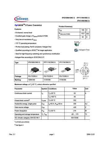
IPB108N15N3 G IPP111N15N3 G IPI111N15N3 G OptiMOSTM3 Power-Transistor Product Summary Features V 150 V DS N-channel, normal level R 10.8 m DS(on),max (TO263) Excellent gate charge x R product (FOM) DS(on) I 83 A D Very low on-resistance R DS(on) 175 C operating temperature Pb-free lead plating; RoHS compliant; Halogen free Qualified according to JE... See More ⇒
Detailed specifications: IPI041N12N3 , IPI051N15N5 , IPI072N10N3 , IPI075N15N3 , IPI076N12N3 , IPI076N15N5 , IPI086N10N3 , IPI100N08N3 , IRFP260N , IPI111N15N3 , IPI147N12N3 , IPI180N10N3 , IPI200N15N3 , IPI200N25N3 , IPI26CN10N , IPI320N20N3 , IPI35CN10N .
Keywords - IPI110N20N3 MOSFET specs
IPI110N20N3 cross reference
IPI110N20N3 equivalent finder
IPI110N20N3 pdf lookup
IPI110N20N3 substitution
IPI110N20N3 replacement
Step-by-step guide to finding a MOSFET replacement. Cross-reference parts and ensure compatibility for your repair or project.


