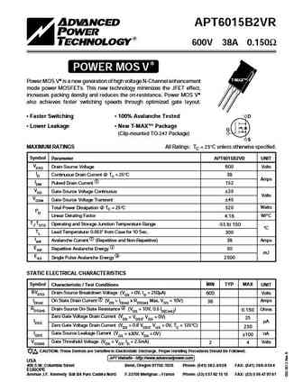
APT6015B2VFR MOSFET Equivalente. Reemplazo. Hoja de especificaciones. Principales características
Número de Parte: APT6015B2VFR
Tipo de FET: MOSFET
Polaridad de transistor: N
ESPECIFICACIONES MÁXIMAS
Pdⓘ - Máxima disipación de potencia: 520 W
|Vds|ⓘ - Voltaje máximo drenador-fuente: 600 V
|Vgs|ⓘ - Voltaje máximo fuente-puerta: 30 V
|Id|ⓘ - Corriente continua de drenaje: 38 A
Tjⓘ - Temperatura máxima de unión: 150 °C
CARACTERÍSTICAS ELÉCTRICAS
trⓘ - Tiempo de subida: 13 nS
Cossⓘ - Capacitancia de salida: 900 pF
RDSonⓘ - Resistencia estado encendido drenaje a fuente: 0.15 Ohm
Encapsulados: TO-247
Búsqueda de reemplazo de APT6015B2VFR MOSFET
- Selecciónⓘ de transistores por parámetros
APT6015B2VFR datasheet
apt6015b2vfr.pdf
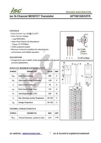
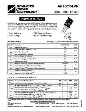
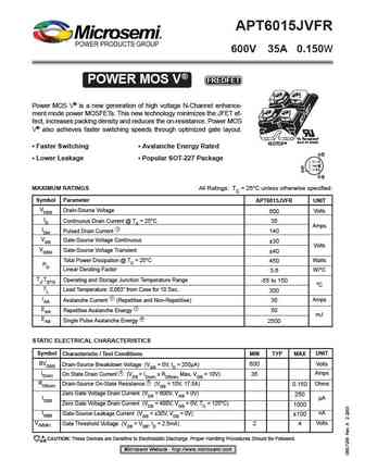
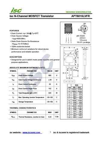
isc N-Channel MOSFET Transistor APT6015B2VFR FEATURES Drain Current I = 38A@ T =25 D C Drain Source Voltage- V =600V(Min) DSS Static Drain-Source On-Resistance R =0.15 (Max) DS(on) 100% avalanche tested Minimum Lot-to-Lot variations for robust device performance and reliable operation DESCRIPTION Designed for use in switch mode power supplies and general pu
apt6015b2vfrg apt6015lvfrg.pdf
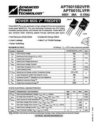
APT6015B2VFR APT6015LVFR 600V 38A 0.150 B2VFR POWER MOS V FREDFET T-MAX TO-264 Power MOS V is a new generation of high voltage N-Channel enhancement mode power MOSFETs. This new technology minimizes the JFET effect, increases packing density and reduces the on-resistance. Power MOS V also achieves faster switching speeds through optimized gate layout.
apt6015b2vr.pdf

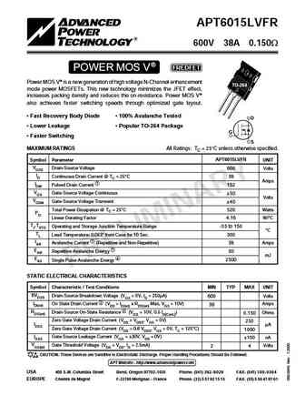
APT6015B2VR 600V 38A 0.150 POWER MOS V T-MAX Power MOS V is a new generation of high voltage N-Channel enhancement mode power MOSFETs. This new technology minimizes the JFET effect, increases packing density and reduces the on-resistance. Power MOS V also achieves faster switching speeds through optimized gate layout. Faster Switching 100% Avalanche Tested D Low
apt6015lvfr.pdf
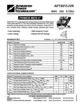
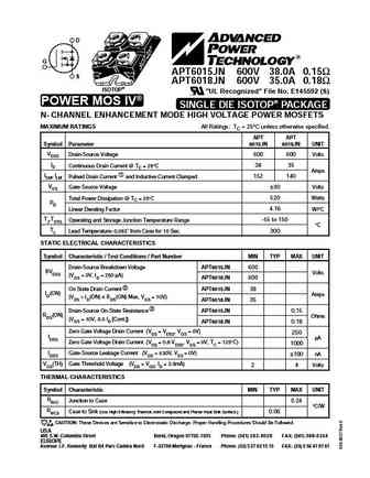
APT6015LVFR 600V 38A 0.150W POWER MOS V FREDFET Power MOS V is a new generation of high voltage N-Channel enhancement TO-264 mode power MOSFETs. This new technology minimizes the JFET effect, increases packing density and reduces the on-resistance. Power MOS V also achieves faster switching speeds through optimized gate layout. Fast Recovery Body Diode 100% Avalanche Teste
Otros transistores... APT5010LFLL , APT5010LLL , APT5015BVFR , APT50M75LFLL , APT50M80LVFR , APT6010B2FLL , APT6010LFLL , APT6013LFLL , IRF1405 , APT6017LFLL , APT60N60BCS , R6004KNJ , R6004KNX , R6007KNJ , R6007KNX , R6007MNJ , R6009JND3 .
History: NTLGD3502N | WSF50N10 | IXFA10N60P | WMM020N10HGS
History: NTLGD3502N | WSF50N10 | IXFA10N60P | WMM020N10HGS
🌐 : EN ES РУ

Liste
Recientemente añadidas las descripciónes de los transistores:
MOSFET: AUB034N10 | AUB033N08BG | AUB026N085 | AUA062N08BG | AUA060N08AG | AUA056N08BGL | AUA039N10 | ASW80R290E | ASW65R120EFD | ASW65R110E | ASW65R095EFD | ASW65R046EFD | ASW65R041EFDA | ASW65R041E | ASW60R150E | ASW60R090EFDA
Popular searches
2n404 | 2n4250 | d882 transistor equivalent | 17n80c3 | bc107 transistor | rjp63g4 datasheet | 2sc1115 | c3998 transistor