APT6015B2VFR Datasheet. Specs and Replacement
Type Designator: APT6015B2VFR 📄📄
Type of Transistor: MOSFET
Type of Control Channel: N-Channel
Absolute Maximum Ratings
Pd ⓘ - Maximum Power Dissipation: 520 W
|Vds|ⓘ - Maximum Drain-Source Voltage: 600 V
|Vgs|ⓘ - Maximum Gate-Source Voltage: 30 V
|Id| ⓘ - Maximum Drain Current: 38 A
Tj ⓘ - Maximum Junction Temperature: 150 °C
Electrical Characteristics
tr ⓘ - Rise Time: 13 nS
Cossⓘ - Output Capacitance: 900 pF
RDSonⓘ - Maximum Drain-Source On-State Resistance: 0.15 Ohm
Package: TO-247
📄📄 Copy
APT6015B2VFR substitution
- MOSFET ⓘ Cross-Reference Search
APT6015B2VFR datasheet
apt6015b2vfr.pdf
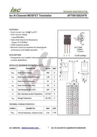
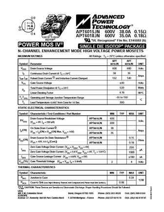
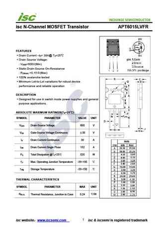
isc N-Channel MOSFET Transistor APT6015B2VFR FEATURES Drain Current I = 38A@ T =25 D C Drain Source Voltage- V =600V(Min) DSS Static Drain-Source On-Resistance R =0.15 (Max) DS(on) 100% avalanche tested Minimum Lot-to-Lot variations for robust device performance and reliable operation DESCRIPTION Designed for use in switch mode power supplies and general pu... See More ⇒
apt6015b2vfrg apt6015lvfrg.pdf
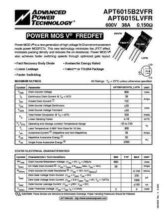
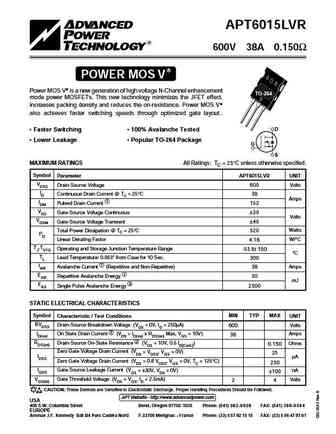
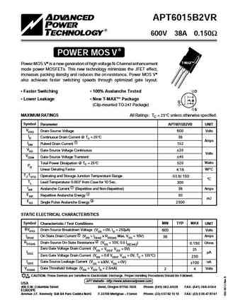
APT6015B2VFR APT6015LVFR 600V 38A 0.150 B2VFR POWER MOS V FREDFET T-MAX TO-264 Power MOS V is a new generation of high voltage N-Channel enhancement mode power MOSFETs. This new technology minimizes the JFET effect, increases packing density and reduces the on-resistance. Power MOS V also achieves faster switching speeds through optimized gate layout. ... See More ⇒
apt6015b2vr.pdf

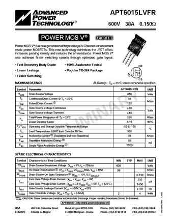
APT6015B2VR 600V 38A 0.150 POWER MOS V T-MAX Power MOS V is a new generation of high voltage N-Channel enhancement mode power MOSFETs. This new technology minimizes the JFET effect, increases packing density and reduces the on-resistance. Power MOS V also achieves faster switching speeds through optimized gate layout. Faster Switching 100% Avalanche Tested D Low... See More ⇒
apt6015lvfr.pdf
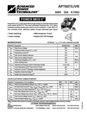
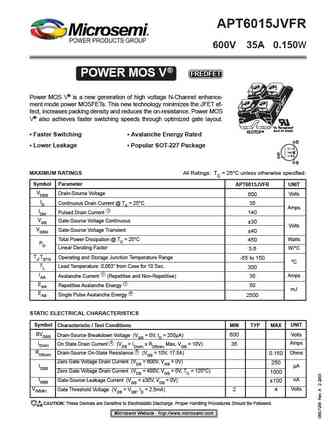
APT6015LVFR 600V 38A 0.150W POWER MOS V FREDFET Power MOS V is a new generation of high voltage N-Channel enhancement TO-264 mode power MOSFETs. This new technology minimizes the JFET effect, increases packing density and reduces the on-resistance. Power MOS V also achieves faster switching speeds through optimized gate layout. Fast Recovery Body Diode 100% Avalanche Teste... See More ⇒
Detailed specifications: APT5010LFLL, APT5010LLL, APT5015BVFR, APT50M75LFLL, APT50M80LVFR, APT6010B2FLL, APT6010LFLL, APT6013LFLL, IRL3713, APT6017LFLL, APT60N60BCS, R6004KNJ, R6004KNX, R6007KNJ, R6007KNX, R6007MNJ, R6009JND3
Keywords - APT6015B2VFR MOSFET specs
APT6015B2VFR cross reference
APT6015B2VFR equivalent finder
APT6015B2VFR pdf lookup
APT6015B2VFR substitution
APT6015B2VFR replacement
Need a MOSFET replacement? Our guide shows you how to find a perfect substitute by comparing key parameters and specs
MOSFET Parameters. How They Affect Each Other
History: FDS5351 | IXFK120N25 | NDB6051
🌐 : EN ES РУ

LIST
Last Update
MOSFET: CS95118 | CS85105A | CS75N45 | CS72N12 | CS55N50 | CS48N75A | CS40N27 | MSQ60P04D | MSQ40P07D | MSQ30P40D
Popular searches
2n404 | 2n4250 | d882 transistor equivalent | 17n80c3 | bc107 transistor | rjp63g4 datasheet | 2sc1115 | c3998 transistor