AS2307 MOSFET Equivalente. Reemplazo. Hoja de especificaciones. Principales características
Número de Parte: AS2307
Tipo de FET: MOSFET
Polaridad de transistor: P
ESPECIFICACIONES MÁXIMAS
Pdⓘ - Máxima disipación de potencia: 1.04 W
|Vds|ⓘ - Voltaje máximo drenador-fuente: 30 V
|Vgs|ⓘ - Voltaje máximo fuente-puerta: 20 V
|Id|ⓘ - Corriente continua de drenaje: 3 A
Tjⓘ - Temperatura máxima de unión: 150 °C
CARACTERÍSTICAS ELÉCTRICAS
trⓘ - Tiempo de subida: 17 nS
Cossⓘ - Capacitancia de salida: 74 pF
RDSonⓘ - Resistencia estado encendido drenaje a fuente: 0.07 Ohm
Encapsulados: SOT23
Búsqueda de reemplazo de AS2307 MOSFET
- Selecciónⓘ de transistores por parámetros
AS2307 datasheet
as2307.pdf
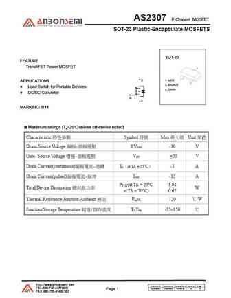
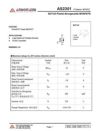
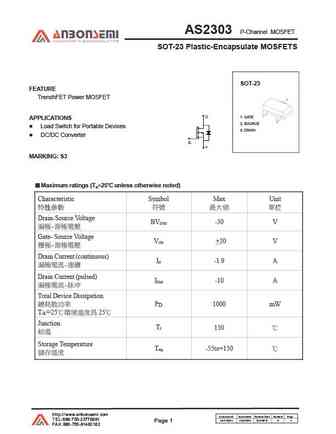
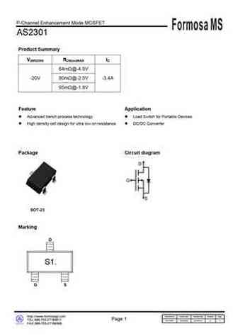
P-Channel MOSFET AS2307 SOT-23 Plastic-Encapsulate MOSFETS SOT-23 FEATURE TrenchFET Power MOSFET 1. GATE APPLICATIONS 2. SOURCE Load Switch for Portable Devices 3. DRAIN DC/DC Converter MARKING B 1 1 Maximum ratings (Ta=25 unless otherwise noted) Characteristic Symbol Max Unit Drain-Source Voltage - BV
as2306.pdf
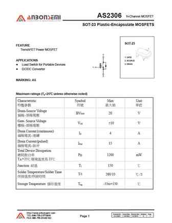
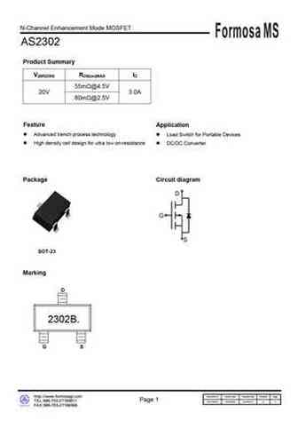
AS2306 N-Channel MOSFET SOT-23 Plastic-Encapsulate MOSFETS SOT-23 FEATURE TrenchFET Power MOSFET 1. GATE APPLICATIONS 2. SOURCE 3. DRAIN Load Switch for Portable Devices DC/DC Converter MARKING A6 Maximum ratings (Ta=25 unless otherwise noted) Characteristic Symbol Max Unit Drain-Source Voltage BV 20 V DSS -
as2302.pdf
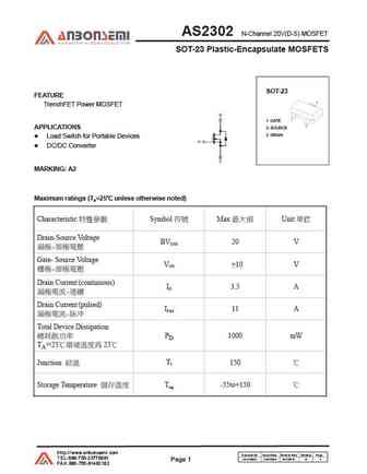
AS2302 N-Channel 20V(D-S) MOSFET SOT-23 Plastic-Encapsulate MOSFETS SOT-23 FEATURE TrenchFET Power MOSFET 1. GATE APPLICATIONS 2. SOURCE 3. DRAIN Load Switch for Portable Devices DC/DC Converter MARKING A2 Maximum ratings (Ta=25 unless otherwise noted) Characteristic Symbol Max Unit Drain-Source Voltage BVDSS 20 V -
as2304.pdf
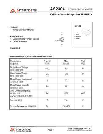
N-Channel 30V(D-S) MOSFET AS2304 SOT-23 Plastic-Encapsulate MOSFETS Dimensions In Millimeters Dimensions In Inches Symbol Min Max Min Max A 0.900 1.150 0.035 0.045 A1 0.000 0.100 0.000 0.004 A2 0.900 1.050 0.035 0.041 b 0.300 0.500 0.012 0.020 c 0.080 0.150 0.003 0.006 D 2.800 3.000 0.110 0.118 E 1.200 1.400 0.047 0.055 E1 2.250 2.550 0.089 0


Otros transistores... AS2101W , AS2102W , AS2300 , AS2301 , AS2302 , AS2303 , AS2304 , AS2305 , 20N60 , BM2300 , BM3402 , BM3407A , BM3415E , BM3416E , BML6401 , BML6402 , SI2301-P .
History: CS25N50AKR | 2SK3111 | IRF720SPBF | AP10TN008CMT-L | MMN400A006U1 | JMH65R980AF | IRF7313PBF-1
History: CS25N50AKR | 2SK3111 | IRF720SPBF | AP10TN008CMT-L | MMN400A006U1 | JMH65R980AF | IRF7313PBF-1
🌐 : EN ES РУ

Liste
Recientemente añadidas las descripciónes de los transistores:
MOSFET: AUB062N08BG | AUB060N08AG | AUB056N10 | AUB056N08BGL | AUB050N085 | AUB050N055 | AUB045N12 | AUB045N10BT | AUB039N10 | AUB034N10 | AUB033N08BG | AUB026N085 | AUA062N08BG | AUA060N08AG | AUA056N08BGL | AUA039N10
Popular searches
2n2905 equivalent | 2sa640 | 2sb527 | 30g124 | 75339p mosfet | a968 transistor | f1010e mosfet | 2sc3883