CEU20N02 MOSFET Equivalente. Reemplazo. Hoja de especificaciones. Principales características
Número de Parte: CEU20N02
Tipo de FET: MOSFET
Polaridad de transistor: N
ESPECIFICACIONES MÁXIMAS
Pdⓘ - Máxima disipación de potencia: 32 W
|Vds|ⓘ - Voltaje máximo drenador-fuente: 20 V
|Vgs|ⓘ - Voltaje máximo fuente-puerta: 12 V
|Id|ⓘ - Corriente continua de drenaje: 18 A
Tjⓘ - Temperatura máxima de unión: 150 °C
CARACTERÍSTICAS ELÉCTRICAS
trⓘ - Tiempo de subida: 13 nS
Cossⓘ - Capacitancia de salida: 220 pF
RDSonⓘ - Resistencia estado encendido drenaje a fuente: 0.042 Ohm
Encapsulados: TO252
Búsqueda de reemplazo de CEU20N02 MOSFET
- Selecciónⓘ de transistores por parámetros
CEU20N02 datasheet
ced20n02 ceu20n02.pdf
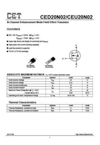
CED20N02/CEU20N02 N-Channel Enhancement Mode Field Effect Transistor FEATURES 20V, 18A, RDS(ON) = 42m @VGS = 4.5V. RDS(ON) = 75m @VGS = 2.5V. Super high dense cell design for extremely low RDS(ON). High power and current handing capability. D Lead free product is acquired. TO-251 & TO-252 package. D G G S CEU SERIES CED SERIES S TO-252(D-PAK) TO-251(I-PAK) ABSOLUTE MAXI
ceu20n06.pdf
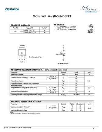
CEU20N06 www.VBsemi.tw N-Channel 6 0-V (D-S) MOSFET FEATURES PRODUCT SUMMARY TrenchFET Power MOSFET VDS (V) rDS(on) ( ) ID (A)a Available 175 C Junction Temperature 0.025 at VGS = 10 V 35 RoHS* 60 0.030 at VGS = 4.5 V 30 COMPLIANT TO-252 D G Drain Connected to Tab G D S S Top View N-Channel MOSFET ABSOLUTE MAXIMUM RATINGS TC = 25 C, unless otherwise no
ced20p10 ceu20p10.pdf
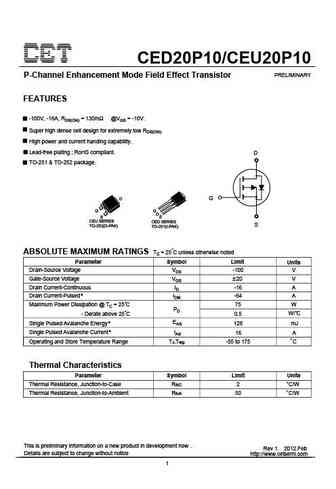
CED20P10/CEU20P10 PRELIMINARY P-Channel Enhancement Mode Field Effect Transistor FEATURES -100V, -16A, RDS(ON) = 130m @VGS = -10V. Super high dense cell design for extremely low RDS(ON). High power and current handing capability. Lead-free plating ; RoHS compliant. D TO-251 & TO-252 package. D G G S CEU SERIES CED SERIES S TO-252(D-PAK) TO-251(I-PAK) ABSOLUTE MAXIMUM RATING
ced20p06 ceu20p06.pdf
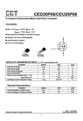
CED20P06/CEU20P06 P-Channel Enhancement Mode Field Effect Transistor FEATURES -60V, -13A, RDS(ON) = 125m @VGS = -10V. RDS(ON) = 175m @VGS = -4.5V. Super high dense cell design for extremely low RDS(ON). High power and current handing capability. D Lead free product is acquired. TO-251 & TO-252 package. D G G S CEU SERIES CED SERIES S TO-252(D-PAK) TO-251(I-PAK) ABSOLUTE
Otros transistores... CJBB3134K , CJBB3139K , CJBD3020 , CJBE5005 , CJBM3020 , CEC2088E , CEC3172 , CED20N02 , AON7506 , CED25N02 , CEU25N02 , CEM2192 , CEM4052 , CEM6056L , CEM9288 , CEN2307A , CEN2321A .
🌐 : EN ES РУ

Liste
Recientemente añadidas las descripciónes de los transistores:
MOSFET: ASD80R750E | ASD70R950E | ASD70R600E | ASD70R380E | ASD65R850E | ASD65R550E | ASD65R350E | ASD65R300E | ASD65R280E | ASD65R270E | ASD60R330E | ASD60R280E | ASB80R750E | ASB70R380E | ASB65R300E | ASB65R220E
Popular searches
bd140 transistor equivalent | tip122 transistor equivalent | irfz44n equivalent | 2n2923 | 2n2102 | mj15003g | oc75 transistor | irfp260m