DMG4N60SK3 MOSFET Equivalente. Reemplazo. Hoja de especificaciones. Principales características
Número de Parte: DMG4N60SK3
Tipo de FET: MOSFET
Polaridad de transistor: N
ESPECIFICACIONES MÁXIMAS
Pdⓘ - Máxima disipación de potencia: 48 W
|Vds|ⓘ - Voltaje máximo drenador-fuente: 600 V
|Vgs|ⓘ - Voltaje máximo fuente-puerta: 30 V
|Id|ⓘ - Corriente continua de drenaje: 3.7 A
Tjⓘ - Temperatura máxima de unión: 150 °C
CARACTERÍSTICAS ELÉCTRICAS
trⓘ - Tiempo de subida: 34 nS
Cossⓘ - Capacitancia de salida: 47 pF
RDSonⓘ - Resistencia estado encendido drenaje a fuente: 2.3 Ohm
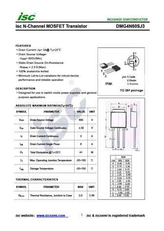
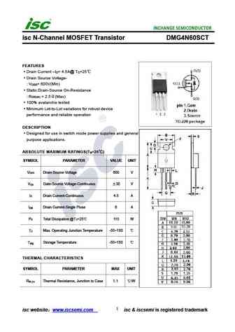
Encapsulados: TO252
Búsqueda de reemplazo de DMG4N60SK3 MOSFET
- Selecciónⓘ de transistores por parámetros
DMG4N60SK3 datasheet
dmg4n60sk3.pdf
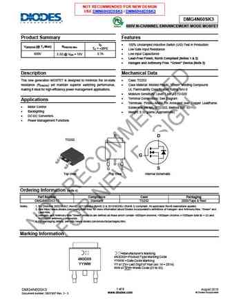
NOT RECOMMENDED FOR NEW DESIGN USE DMN60H3D5SK3 / DMN60H4D5SK3 DMG4N60SK3 600V N-CHANNEL ENHANCEMENT MODE MOSFET Product Summary Features ID 100% Unclamped Inductive Switch (UIS) Test in Production V(BR)DSS (@ TJ Max) RDS(ON) Max TC = +25 C Low Gate Input Resistance 650V 3.7A Low Input Capacitance 2.3 @ VGS = 10V Lead-Free Finish; RoHS Compliant (Note
dmg4n60sk3.pdf
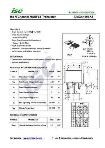
isc N-Channel MOSFET Transistor DMG4N60SK3 FEATURES Drain Current I = 3.7A@ T =25 D C Drain Source Voltage- V = 600V(Min) DSS Static Drain-Source On-Resistance R = 2.3 (Max) DS(on) 100% avalanche tested Minimum Lot-to-Lot variations for robust device performance and reliable operation DESCRIPTION Designed for use in switch mode power supplies and general pu
dmg4n60sj3.pdf
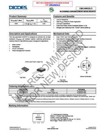
NOT RECOMMENDED FOR NEW DESIGN USE DMG3N60SJ3 DMG4N60SJ3 N-CHANNEL ENHANCEMENT MODE MOSFET Product Summary Features and Benefits ID Low On-Resistance BVDSS (@ TJ Max) RDS(ON) Max TC = +25 C High BVDSS Rating for Power Application 650V 3.0A Low Input Capacitance 2.5 @ VGS = 10V Lead-Free Finish; RoHS Compliant (Notes 1 & 2) Halogen and Antimony F
dmg4n60sct.pdf
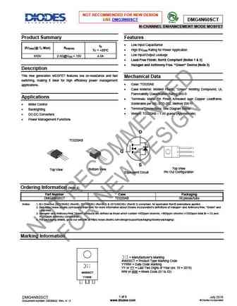
NOT RECOMMENDED FOR NEW DESIGN USE DMG3N60SCT DMG4N60SCT N-CHANNEL ENHANCEMENT MODE MOSFET Product Summary Features Low Input Capacitance ID BVDSS (@ TJ Max) RDS(ON) High BVDSS Rating for Power Application TC = +25 C Low Input/Output Leakage 650V 2.5 @VGS = 10V 4.5A Lead-Free Finish; RoHS Compliant (Notes 1 & 2) Halogen and Antimony Free. Gre
Otros transistores... DMTH8012LPSW , ZXMP10A13FQ , ZXMS6005DGQ-13 , 19N20 , DMG10N60SCT , DMG3N60SJ3 , DMG4N60SCT , DMG4N60SJ3 , 7N60 , DMG7N65SCT , DMG7N65SCTI , DMG7N65SJ3 , DMG8N65SCT , DMJ70H1D0SV3 , DMJ70H1D3SH3 , DMJ70H1D4SV3 , DMJ70H1D5SV3 .
🌐 : EN ES РУ

Liste
Recientemente añadidas las descripciónes de los transistores:
MOSFET: AUB034N10 | AUB033N08BG | AUB026N085 | AUA062N08BG | AUA060N08AG | AUA056N08BGL | AUA039N10 | ASW80R290E | ASW65R120EFD | ASW65R110E | ASW65R095EFD | ASW65R046EFD | ASW65R041EFDA | ASW65R041E | ASW60R150E | ASW60R090EFDA
Popular searches
irf3205 | irfz44n datasheet | 2n4401 | bc547 transistor | bd139 | 2n4401 datasheet | irf640 | irf840