SSS4N90AS MOSFET Equivalente. Reemplazo. Hoja de especificaciones. Principales características
Número de Parte: SSS4N90AS
Tipo de FET: MOSFET
Polaridad de transistor: N
ESPECIFICACIONES MÁXIMAS
Pdⓘ - Máxima disipación de potencia: 40 W
|Vds|ⓘ - Voltaje máximo drenador-fuente: 900 V
|Vgs|ⓘ - Voltaje máximo fuente-puerta: 30 V
|Id|ⓘ - Corriente continua de drenaje: 2.8 A
Tjⓘ - Temperatura máxima de unión: 150 °C
CARACTERÍSTICAS ELÉCTRICAS
trⓘ - Tiempo de subida: 31 nS
Cossⓘ - Capacitancia de salida: 85 pF
RDSonⓘ - Resistencia estado encendido drenaje a fuente: 3.7 Ohm
Encapsulados: TO220F
Búsqueda de reemplazo de SSS4N90AS MOSFET
- Selecciónⓘ de transistores por parámetros
SSS4N90AS datasheet
sss4n90as.pdf
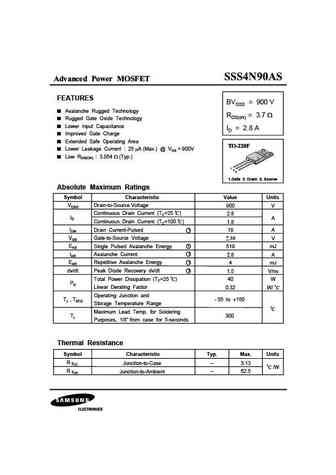
Advanced Power MOSFET FEATURES BVDSS = 900 V Avalanche Rugged Technology RDS(on) = 3.7 Rugged Gate Oxide Technology Lower Input Capacitance ID = 2.8 A Improved Gate Charge Extended Safe Operating Area Lower Leakage Current 25 A (Max.) @ VDS = 900V Low RDS(ON) 3.054 (Typ.) 1 2 3 1.Gate 2. Drain 3. Source Absolute Maximum Ratings Symbol Characteristic Valu
sss4n90a.pdf

Advanced Power MOSFET FEATURES BVDSS = 900 V Avalanche Rugged Technology RDS(on) = 5.0 Rugged Gate Oxide Technology Lower Input Capacitance ID = 2.5 A Improved Gate Charge Extended Safe Operating Area Lower Leakage Current 25 A (Max.) @ VDS = 900V Low RDS(ON) 4.181 (Typ.) 1 2 3 1.Gate 2. Drain 3. Source Absolute Maximum Ratings Symbol Characteristic Valu
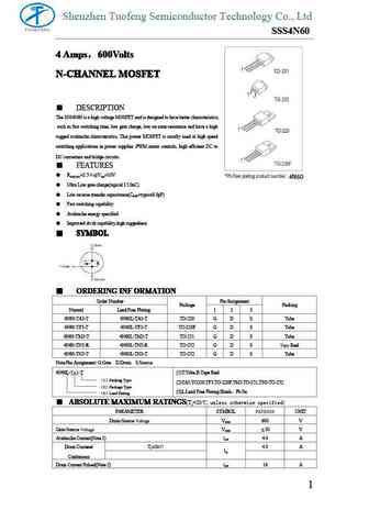
ssp4n60b sss4n60b.pdf
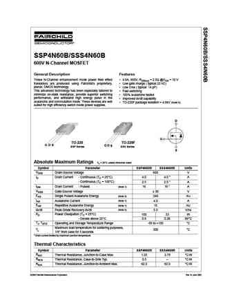
SSP4N60B/SSS4N60B 600V N-Channel MOSFET General Description Features These N-Channel enhancement mode power field effect 4.0A, 600V, RDS(on) = 2.5 @VGS = 10 V transistors are produced using Fairchild s proprietary, Low gate charge ( typical 22 nC) planar, DMOS technology. Low Crss ( typical 14 pF) This advanced technology has been especially tailored to Fast switchi
sss4n80as.pdf
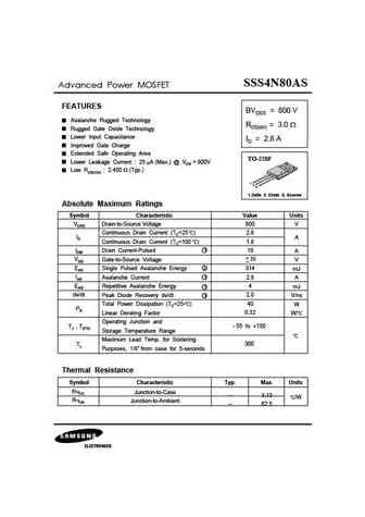
SSS4N80AS Advanced Power MOSFET FEATURES BVDSS = 800 V Avalanche Rugged Technology RDS(on) = 3.0 Rugged Gate Oxide Technology Lower Input Capacitance ID = 2.8 A Improved Gate Charge Extended Safe Operating Area TO-220F Lower Leakage Current 25 A (Max.) @ VDS = 800V Low RDS(ON) 2.450 (Typ.) 1 2 3 1.Gate 2. Drain 3. Source Absolute Maximum Ratings Symbol C


Otros transistores... SSS3N80A , SSS3N90A , SSS4N55 , SSS4N60 , SSS4N60AS , SSS4N80A , SSS4N80AS , SSS4N90A , 8205A , SSS5N80A , SSS5N90A , SSS6N55 , SSS6N60 , SSS6N70A , SSS6N80A , SSS6N90A , SSS70N10A .
🌐 : EN ES РУ

Liste
Recientemente añadidas las descripciónes de los transistores:
MOSFET: AOSS62934 | AOSN21319C | AONS66966 | AONR62992 | AON7400B | AON6578 | AO3480C | AO3400C | HAF1008S | HAF1008L | EMZB08P03H | CS30N20FA9R | AOT66613L | AOSP21313C | AOSP21311C | AOB66918L
Popular searches
d882p | 2sb1560 | 2n1304 | 2sa979 | 2sc4793 | d965 | mje15031 | irfp150n