NVTFS9D6P04M8L MOSFET Equivalente. Reemplazo. Hoja de especificaciones. Principales características
Número de Parte: NVTFS9D6P04M8L
Tipo de FET: MOSFET
Polaridad de transistor: P
ESPECIFICACIONES MÁXIMAS
Pdⓘ - Máxima disipación de potencia: 75 W|Vds|ⓘ - Voltaje máximo drenador - fuente: 40 V
|Vgs|ⓘ - Voltaje máximo fuente - puerta: 20 V
|Id|ⓘ - Corriente continua de drenaje: 64 A
Tjⓘ - Temperatura máxima de unión: 175 °C
CARACTERÍSTICAS ELÉCTRICAS
trⓘ - Tiempo de subida: 91.5 nS
Cossⓘ - Capacitancia de salida: 923 pF
Rds(on)ⓘ - Resistencia estado encendido drenaje a fuente: 0.0095 Ohm
Paquete / Cubierta: WDFN8
Búsqueda de reemplazo de NVTFS9D6P04M8L MOSFET
NVTFS9D6P04M8L datasheet
nvtfs9d6p04m8l.pdf
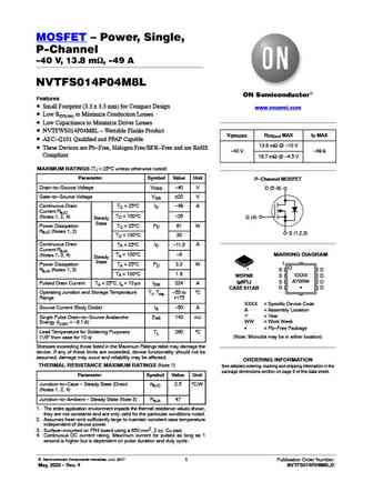
MOSFET - Power, Single P-Channel -40 V, 9.5 mW, -64 A NVTFS9D6P04M8L Features Small Footprint (3.3 x 3.3 mm) for Compact Design www.onsemi.com Low RDS(on) to Minimize Conduction Losses Low Capacitance to Minimize Driver Losses NVTFWS9D6P04M8L - Wettable Flanks Product V(BR)DSS RDS(on) MAX ID MAX AEC-Q101 Qualified and PPAP Capable 9.5 mW @ -10 V These Device
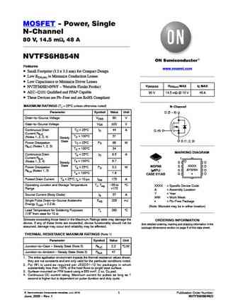
nvtfs6h854n.pdf
MOSFET - Power, Single N-Channel 80 V, 14.5 mW, 48 A NVTFS6H854N Features www.onsemi.com Small Footprint (3.3 x 3.3 mm) for Compact Design Low RDS(on) to Minimize Conduction Losses Low Capacitance to Minimize Driver Losses V(BR)DSS RDS(on) MAX ID MAX NVTFS6H854NWF - Wettable Flanks Product AEC-Q101 Qualified and PPAP Capable 80 V 14.5 mW @ 10 V 48 A These De
nvtfs6h860n.pdf
MOSFET - Power, Single N-Channel 80 V, 21.1 mW, 33 A NVTFS6H860N Features www.onsemi.com Small Footprint (3.3 x 3.3 mm) for Compact Design Low RDS(on) to Minimize Conduction Losses Low Capacitance to Minimize Driver Losses V(BR)DSS RDS(on) MAX ID MAX NVTFS6H860NWF - Wettable Flanks Product AEC-Q101 Qualified and PPAP Capable 80 V 21.1 mW @ 10 V 33 A These De
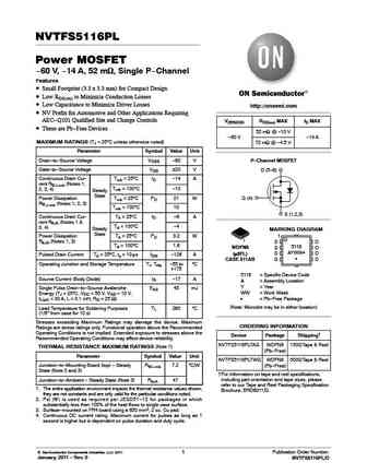
nvtfs5116pl-d.pdf
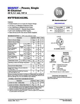
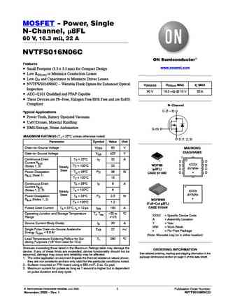
NVTFS5116PL Power MOSFET -60 V, -14 A, 52 mW, Single P-Channel Features Small Footprint (3.3 x 3.3 mm) for Compact Design Low RDS(on) to Minimize Conduction Losses Low Capacitance to Minimize Driver Losses http //onsemi.com NV Prefix for Automotive and Other Applications Requiring AEC-Q101 Qualified Site and Change Controls V(BR)DSS RDS(on) MAX ID MAX These are Pb
nvtfs002n04c.pdf
NVTFS002N04C MOSFET Power, Single N-Channel 40 V, 2.4 mW, 136 A Features www.onsemi.com Small Footprint (3.3 x 3.3 mm) for Compact Design Low RDS(on) to Minimize Conduction Losses Low Capacitance to Minimize Driver Losses NVTFWS002N04C - Wettable Flanks Product V(BR)DSS RDS(on) MAX ID MAX AEC-Q101 Qualified and PPAP Capable 40 V 2.4 mW @ 10 V 136 A These
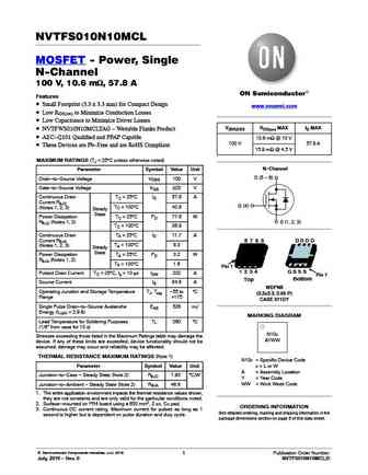
nvtfs010n10mcl.pdf
NVTFS010N10MCL MOSFET - Power, Single N-Channel 100 V, 10.6 mW, 57.8 A Features Small Footprint (3.3 x 3.3 mm) for Compact Design www.onsemi.com Low RDS(on) to Minimize Conduction Losses Low Capacitance to Minimize Driver Losses V(BR)DSS RDS(on) MAX ID MAX NVTFWS010N10MCLTAG - Wettable Flanks Product AEC-Q101 Qualified and PPAP Capable 10.6 mW @ 10 V 100 V 57.8
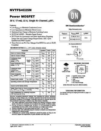
nvtfs4c25n.pdf
NVTFS4C25N Power MOSFET 30 V, 17 mW, 22 A, Single N-Channel, m8FL Features Low RDS(on) to Minimize Conduction Losses http //onsemi.com Low Capacitance to Minimize Driver Losses Optimized Gate Charge to Minimize Switching Losses V(BR)DSS RDS(on) MAX ID MAX NVTFS4C25NWF - Wettable Flanks Product 17 mW @ 10 V NVT Prefix for Automotive and Other Applications Requiring
nvtfs5c453nl.pdf
MOSFET Power, Single N-Channel 40 V, 3.1 mW, 107 A NVTFS5C453NL Features www.onsemi.com Small Footprint (3.3 x 3.3 mm) for Compact Design Low RDS(on) to Minimize Conduction Losses Low Capacitance to Minimize Driver Losses V(BR)DSS RDS(ON) MAX ID MAX NVTFS5C453NLWF - Wettable Flanks Product 3.1 mW @ 10 V 40 V 107 A AEC-Q101 Qualified and PPAP Capable 5.2 mW
nvtfs4c06n.pdf
NVTFS4C06N Power MOSFET 30 V, 4.2 mW, 71 A, Single N-Channel, m8FL Features Low RDS(on) to Minimize Conduction Losses Low Capacitance to Minimize Driver Losses http //onsemi.com Optimized Gate Charge to Minimize Switching Losses NVTFS4C06NWF - Wettable Flanks Product V(BR)DSS RDS(on) MAX ID MAX NVT Prefix for Automotive and Other Applications Requiring 4.2 mW @ 1
nvtfs003n04c.pdf
NVTFS003N04C MOSFET Power, Single N-Channel 40 V, 3.5 mW, 103 A Features www.onsemi.com Small Footprint (3.3 x 3.3 mm) for Compact Design Low RDS(on) to Minimize Conduction Losses Low Capacitance to Minimize Driver Losses NVTFWS003N04C - Wettable Flanks Product V(BR)DSS RDS(on) MAX ID MAX AEC-Q101 Qualified and PPAP Capable 40 V 3.5 mW @ 10 V 103 A These
nvtfs6h880nl.pdf
MOSFET - Power, Single N-Channel 80 V, 29 mW, 22 A NVTFS6H880NL Features Small Footprint (3.3 x 3.3 mm) for Compact Design www.onsemi.com Low RDS(on) to Minimize Conduction Losses Low Capacitance to Minimize Driver Losses V(BR)DSS RDS(ON) MAX ID MAX NVTFS6H880NLWF - Wettable Flanks Product AEC-Q101 Qualified and PPAP Capable 29 mW @ 10 V 80 V 22 A These Devi
nvtfs5826nl-d.pdf
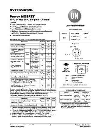
NVTFS5826NL Power MOSFET 60 V, 24 mW, 20 A, Single N-Channel Features Small Footprint (3.3 x 3.3 mm) for Compact Design Low RDS(on) to Minimize Conduction Losses Low Capacitance to Minimize Driver Losses http //onsemi.com NV Prefix for Automotive and Other Applications Requiring AEC-Q101 Qualified Site and Change Controls V(BR)DSS RDS(on) MAX ID MAX These are Pb-F
nvtfs5c680nl.pdf
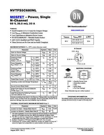
NVTFS5C680NL MOSFET Power, Single N-Channel 60 V, 26.5 mW, 20 A Features www.onsemi.com Small Footprint (3.3 x 3.3 mm) for Compact Design Low RDS(on) to Minimize Conduction Losses Low Capacitance to Minimize Driver Losses V(BR)DSS RDS(on) MAX ID MAX NVTFS5C680NLWF - Wettable Flanks Product 26.5 mW @ 10 V AEC-Q101 Qualified and PPAP Capable 60 V 20 A The
nvtfs4824n.pdf
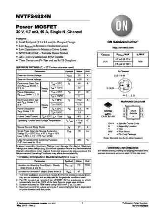
NVTFS4824N Power MOSFET 30 V, 4.7 mW, 46 A, Single N-Channel Features Small Footprint (3.3 x 3.3 mm) for Compact Design Low RDS(on) to Minimize Conduction Losses http //onsemi.com Low Capacitance to Minimize Driver Losses NVTFS4824NWF - Wettable Flanks Product V(BR)DSS RDS(on) MAX ID MAX AEC-Q101 Qualified and PPAP Capable 4.7 mW @ 10 V These Devices are Pb-F
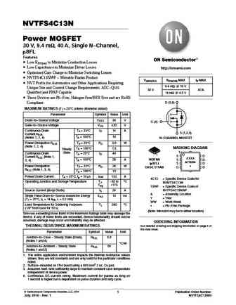
nvtfs4c13n.pdf
NVTFS4C13N Power MOSFET 30 V, 9.4 mW, 40 A, Single N-Channel, m8FL Features Low RDS(on) to Minimize Conduction Losses Low Capacitance to Minimize Driver Losses http //onsemi.com Optimized Gate Charge to Minimize Switching Losses NVTFS4C13NWF - Wettable Flanks Product V(BR)DSS RDS(ON) MAX ID MAX NVT Prefix for Automotive and Other Applications Requiring 9.4 mW @ 1
nvtfs5c454nl.pdf
NVTFS5C454NL Power MOSFET 40 V, 4.0 mW, 85 A, Single N-Channel Features Small Footprint (3.3 x 3.3 mm) for Compact Design Low RDS(on) to Minimize Conduction Losses www.onsemi.com Low Capacitance to Minimize Driver Losses NVTFS5C454NLWF - Wettable Flanks Product AEC-Q101 Qualified and PPAP Capable V(BR)DSS RDS(on) MAX ID MAX These Devices are Pb-Free and are Ro
nvtfs015n04c.pdf
NVTFS015N04C MOSFET Power, Single N-Channel 40 V, 17.3 mW, 27 A Features www.onsemi.com Small Footprint (3.3 x 3.3 mm) for Compact Design Low RDS(on) to Minimize Conduction Losses Low Capacitance to Minimize Driver Losses NVTFWS015N04C - Wettable Flanks Product V(BR)DSS RDS(on) MAX ID MAX AEC-Q101 Qualified and PPAP Capable 40 V 17.3 mW @ 10 V 27 A These
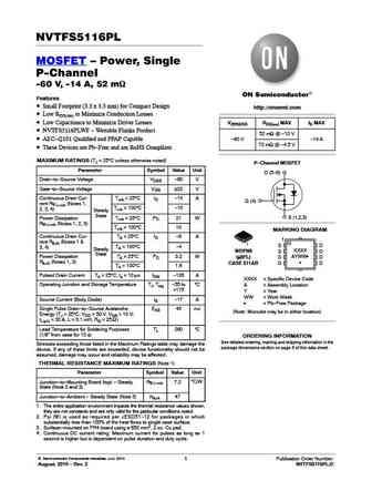
nvtfs5116pl.pdf
NVTFS5116PL MOSFET Power, Single P-Channel -60 V, -14 A, 52 mW Features Small Footprint (3.3 x 3.3 mm) for Compact Design http //onsemi.com Low RDS(on) to Minimize Conduction Losses Low Capacitance to Minimize Driver Losses V(BR)DSS RDS(on) MAX ID MAX NVTFS5116PLWF - Wettable Flanks Product 52 mW @ -10 V -60 V -14 A AEC-Q101 Qualified and PPAP Capable 72 mW
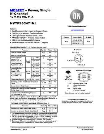
nvtfs5c471nl.pdf
MOSFET Power, Single N-Channel 40 V, 9.0 mW, 41 A NVTFS5C471NL Features www.onsemi.com Small Footprint (3.3 x 3.3 mm) for Compact Design Low RDS(on) to Minimize Conduction Losses Low Capacitance to Minimize Driver Losses V(BR)DSS RDS(on) MAX ID MAX NVTFS5C471NLWF - Wettable Flanks Product 9.0 mW @ 10 V AEC-Q101 Qualified and PPAP Capable 40 V 41 A These
nvtfs4c08n.pdf
NVTFS4C08N Power MOSFET 30 V, 5.9 mW, 55 A, Single N-Channel, m8FL Features Low RDS(on) to Minimize Conduction Losses Low Capacitance to Minimize Driver Losses http //onsemi.com Optimized Gate Charge to Minimize Switching Losses NVTFS4C08NWF - Wettable Flanks Product V(BR)DSS RDS(on) MAX ID MAX NVT Prefix for Automotive and Other Applications Requiring 5.9 mW @ 1
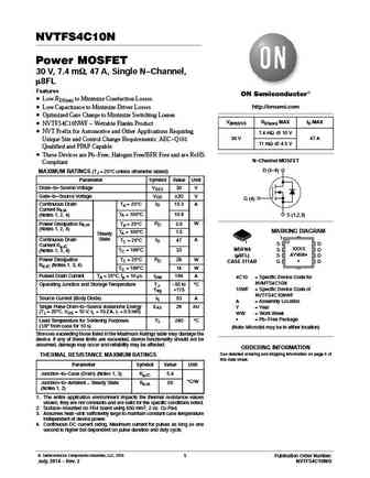
nvtfs4c10n.pdf
NVTFS4C10N Power MOSFET 30 V, 7.4 mW, 47 A, Single N-Channel, m8FL Features Low RDS(on) to Minimize Conduction Losses http //onsemi.com Low Capacitance to Minimize Driver Losses Optimized Gate Charge to Minimize Switching Losses V(BR)DSS RDS(on) MAX ID MAX NVTFS4C10NWF - Wettable Flanks Product NVT Prefix for Automotive and Other Applications Requiring 7.4 mW @ 1
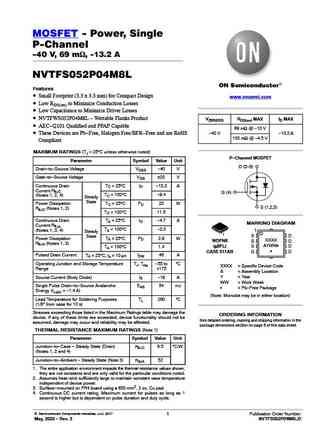
nvtfs052p04m8l.pdf
MOSFET - Power, Single P-Channel -40 V, 69 mW, -13.2 A NVTFS052P04M8L Features Small Footprint (3.3 x 3.3 mm) for Compact Design www.onsemi.com Low RDS(on) to Minimize Conduction Losses Low Capacitance to Minimize Driver Losses NVTFWS052P04M8L - Wettable Flanks Product V(BR)DSS RDS(on) MAX ID MAX AEC-Q101 Qualified and PPAP Capable 69 mW @ -10 V These Device
nvtfs008n04c.pdf
NVTFS008N04C Power MOSFET 40 V, 7.1 mW, 48 A, Single N-Channel Features Small Footprint (3.3 x 3.3 mm) for Compact Design Low RDS(on) to Minimize Conduction Losses www.onsemi.com Low Capacitance to Minimize Driver Losses NVTFWS008N04C - Wettable Flanks Product AEC-Q101 Qualified and PPAP Capable V(BR)DSS RDS(on) MAX ID MAX These Devices are Pb-Free and are RoH
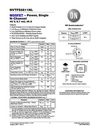
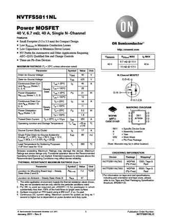
nvtfs5811nl.pdf
NVTFS5811NL MOSFET Power, Single N-Channel 40 V, 6.7 mW, 40 A Features Small Footprint (3.3 x 3.3 mm) for Compact Design http //onsemi.com Low RDS(on) to Minimize Conduction Losses Low Capacitance to Minimize Driver Losses V(BR)DSS RDS(on) MAX ID MAX NVTFS5811NLWF - Wettable Flanks Product AEC-Q101 Qualified and PPAP Capable 6.7 mW @ 10 V 40 V 40 A These
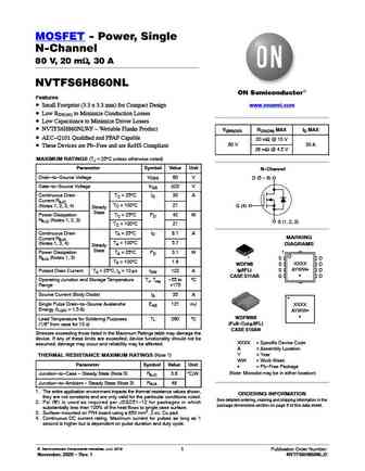
nvtfs6h860nl.pdf
MOSFET - Power, Single N-Channel 80 V, 20 mW, 30 A NVTFS6H860NL Features Small Footprint (3.3 x 3.3 mm) for Compact Design www.onsemi.com Low RDS(on) to Minimize Conduction Losses Low Capacitance to Minimize Driver Losses NVTFS6H860NLWF - Wettable Flanks Product V(BR)DSS RDS(ON) MAX ID MAX AEC-Q101 Qualified and PPAP Capable 20 mW @ 10 V 80 V 30 A These Devi
nvtfs6h880n.pdf
MOSFET - Power, Single N-Channel 80 V, 32 mW, 22 A NVTFS6H880N Features www.onsemi.com Small Footprint (3.3 x 3.3 mm) for Compact Design Low RDS(on) to Minimize Conduction Losses Low Capacitance to Minimize Driver Losses V(BR)DSS RDS(on) MAX ID MAX NVTFS6H880NWF - Wettable Flanks Product AEC-Q101 Qualified and PPAP Capable 80 V 32 mW @ 10 V 22 A These Device
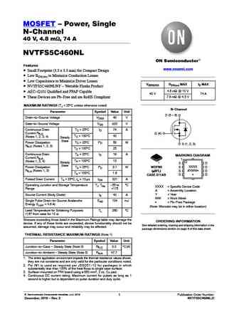
nvtfs5c460nl.pdf
MOSFET Power, Single N-Channel 40 V, 4.8 mW, 74 A NVTFS5C460NL Features www.onsemi.com Small Footprint (3.3 x 3.3 mm) for Compact Design Low RDS(on) to Minimize Conduction Losses Low Capacitance to Minimize Driver Losses V(BR)DSS RDS(on) MAX ID MAX NVTFS5C460NLWF - Wettable Flanks Product 4.8 mW @ 10 V AEC-Q101 Qualified and PPAP Capable 40 V 74 A These
nvtfs4c05n.pdf
NVTFS4C05N Power MOSFET 30 V, 3.6 mW, 102 A, Single N-Channel, m8FL Features Low RDS(on) to Minimize Conduction Losses Low Capacitance to Minimize Driver Losses http //onsemi.com Optimized Gate Charge to Minimize Switching Losses NVTFS4C05NWF - Wettable Flanks Product V(BR)DSS RDS(on) MAX ID MAX NVT Prefix for Automotive and Other Applications Requiring 3.6 mW @
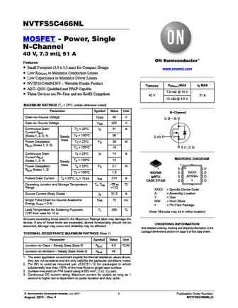
nvtfs5c466nl.pdf
NVTFS5C466NL MOSFET - Power, Single N-Channel 40 V, 7.3 mW, 51 A Features Small Footprint (3.3 x 3.3 mm) for Compact Design www.onsemi.com Low RDS(on) to Minimize Conduction Losses Low Capacitance to Minimize Driver Losses NVTFS5C466NLWF - Wettable Flanks Product V(BR)DSS RDS(on) MAX ID MAX AEC-Q101 Qualified and PPAP Capable 7.3 mW @ 10 V These Devices are
nvtfs5826nl.pdf
NVTFS5826NL Power MOSFET 60 V, 24 mW, 20 A, Single N-Channel Features Small Footprint (3.3 x 3.3 mm) for Compact Design Low RDS(on) to Minimize Conduction Losses http //onsemi.com Low Capacitance to Minimize Driver Losses NVTFS5826NLWF - Wettable Flanks Product V(BR)DSS RDS(on) MAX ID MAX AEC-Q101 Qualified and PPAP Capable 24 mW @ 10 V These Devices are Pb-F
nvtfs5811nl-d.pdf
NVTFS5811NL Power MOSFET 40 V, 6.7 mW, 40 A, Single N-Channel Features Small Footprint (3.3 x 3.3 mm) for Compact Design Low RDS(on) to Minimize Conduction Losses Low Capacitance to Minimize Driver Losses http //onsemi.com NV Prefix for Automotive and Other Applications Requiring AEC-Q101 Qualified Site and Change Controls V(BR)DSS RDS(on) MAX ID MAX These are Pb-
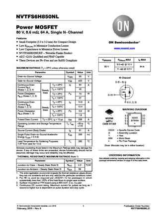
nvtfs6h850nl.pdf
NVTFS6H850NL Power MOSFET 80 V, 8.6 mW, 64 A, Single N-Channel Features Small Footprint (3.3 x 3.3 mm) for Compact Design Low RDS(on) to Minimize Conduction Losses www.onsemi.com Low Capacitance to Minimize Driver Losses NVTFS6H850NLWF - Wettable Flanks Product AEC-Q101 Qualified and PPAP Capable V(BR)DSS RDS(on) MAX ID MAX These Devices are Pb-Free and are Ro
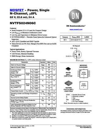
nvtfs024n06c.pdf
MOSFET - Power, Single N-Channel, m8FL 60 V, 22.6 mW, 24 A NVTFS024N06C Features www.onsemi.com Small Footprint (3.3 x 3.3 mm) for Compact Design Low RDS(on) to Minimize Conduction Losses Low QG and Capacitance to Minimize Driver Losses V(BR)DSS RDS(on) MAX ID MAX NVTFWS024N06C - Wettable Flank Option for Enhanced Optical Inspection 60 V 22.6 mW @ 10 V 24 A AEC-
nvtfs6h854nl.pdf
MOSFET - Power, Single N-Channel 80 V, 13.4 mW, 41 A NVTFS6H854NL Features Small Footprint (3.3 x 3.3 mm) for Compact Design www.onsemi.com Low RDS(on) to Minimize Conduction Losses Low Capacitance to Minimize Driver Losses NVTFS6H854NLWF - Wettable Flanks Product V(BR)DSS RDS(ON) MAX ID MAX AEC-Q101 Qualified and PPAP Capable 13.4 mW @ 10 V These Devices ar
nvtfs005n04c.pdf
NVTFS005N04C Power MOSFET 40 V, 5.6 mW, 69 A, Single N-Channel Features Small Footprint (3.3 x 3.3 mm) for Compact Design Low RDS(on) to Minimize Conduction Losses www.onsemi.com Low Capacitance to Minimize Driver Losses NVTFWS005N04C - Wettable Flanks Product AEC-Q101 Qualified and PPAP Capable V(BR)DSS RDS(on) MAX ID MAX These Devices are Pb-Free and are RoH
nvtfs016n06c.pdf
MOSFET - Power, Single N-Channel, m8FL 60 V, 16.3 mW, 32 A NVTFS016N06C Features www.onsemi.com Small Footprint (3.3 x 3.3 mm) for Compact Design Low RDS(on) to Minimize Conduction Losses Low QG and Capacitance to Minimize Driver Losses NVTFWS016N06C - Wettable Flank Option for Enhanced Optical V(BR)DSS RDS(on) MAX ID MAX Inspection 60 V 16.3 mW @ 10 V 32 A AEC-
nvtfs5124pl.pdf
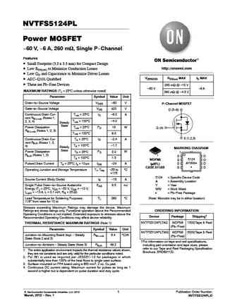
NVTFS5124PL Power MOSFET -60 V, -6 A, 260 mW, Single P-Channel Features Small Footprint (3.3 x 3.3 mm) for Compact Design http //onsemi.com Low RDS(on) to Minimize Conduction Losses Low QG and Capacitance to Minimize Driver Losses V(BR)DSS RDS(on) MAX ID MAX AEC-Q101 Qualified These are Pb-Free Devices 260 mW @ -10 V -60 V -6 A MAXIMUM RATINGS (TJ = 25 C unless
nvtfs014p04m8l.pdf
MOSFET Power, Single, P-Channel -40 V, 13.8 mW, -49 A NVTFS014P04M8L Features Small Footprint (3.3 x 3.3 mm) for Compact Design www.onsemi.com Low RDS(on) to Minimize Conduction Losses Low Capacitance to Minimize Driver Losses NVTFWS014P04M8L - Wettable Flanks Product V(BR)DSS RDS(on) MAX ID MAX AEC-Q101 Qualified and PPAP Capable 13.8 mW @ -10 V These D
nvtfs030n06c.pdf
MOSFET - Power, Single N-Channel, m8FL 60 V, 29.7 mW, 19 A NVTFS030N06C Features www.onsemi.com Small Footprint (3.3 x 3.3 mm) for Compact Design Low RDS(on) to Minimize Conduction Losses Low QG and Capacitance to Minimize Driver Losses NVTFWS030N06C - Wettable Flank Option for Enhanced Optical V(BR)DSS RDS(on) MAX ID MAX Inspection 60 V 29.7 mW @ 10 V 19 A AEC-
nvtfs5c673nl.pdf
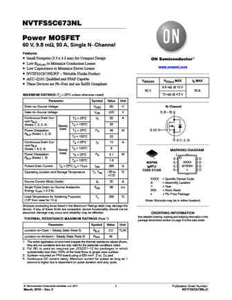
NVTFS5C673NL Power MOSFET 60 V, 9.8 mW, 50 A, Single N-Channel Features Small Footprint (3.3 x 3.3 mm) for Compact Design Low RDS(on) to Minimize Conduction Losses www.onsemi.com Low Capacitance to Minimize Driver Losses NVTFS5C673NLWF - Wettable Flanks Product AEC-Q101 Qualified and PPAP Capable V(BR)DSS RDS(on) MAX ID MAX These Devices are Pb-Free and are Ro
nvtfs5c670nl.pdf
NVTFS5C670NL Power MOSFET 60 V, 6.8 mW, 70 A, Single N-Channel Features Small Footprint (3.3 x 3.3 mm) for Compact Design Low RDS(on) to Minimize Conduction Losses www.onsemi.com Low Capacitance to Minimize Driver Losses NVTFS5C670NLWF - Wettable Flanks Product AEC-Q101 Qualified and PPAP Capable V(BR)DSS RDS(on) MAX ID MAX These Devices are Pb-Free and are Ro
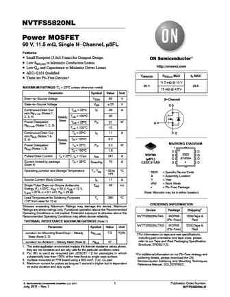
nvtfs5820nl-d.pdf
NVTFS5820NL Power MOSFET 60 V, 11.5 mW, Single N-Channel, m8FL Features Small Footprint (3.3x3.3 mm) for Compact Design Low RDS(on) to Minimize Conduction Losses http //onsemi.com Low QG and Capacitance to Minimize Driver Losses AEC-Q101 Qualified V(BR)DSS RDS(on) MAX ID MAX These are Pb-Free Devices* 11.5 mW @ 10 V 60 V 29 A MAXIMUM RATINGS (TJ = 25 C unless o
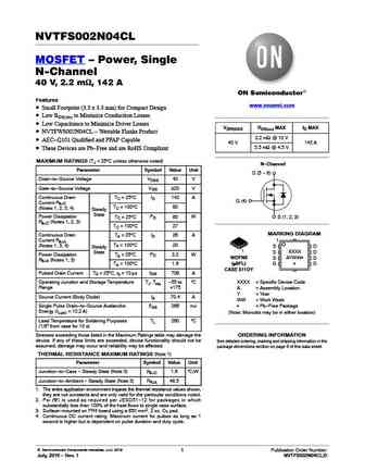
nvtfs002n04cl.pdf
NVTFS002N04CL MOSFET Power, Single N-Channel 40 V, 2.2 mW, 142 A Features www.onsemi.com Small Footprint (3.3 x 3.3 mm) for Compact Design Low RDS(on) to Minimize Conduction Losses Low Capacitance to Minimize Driver Losses V(BR)DSS RDS(on) MAX ID MAX NVTFWS002N04CL - Wettable Flanks Product 2.2 mW @ 10 V AEC-Q101 Qualified and PPAP Capable 40 V 142 A 3.5 mW
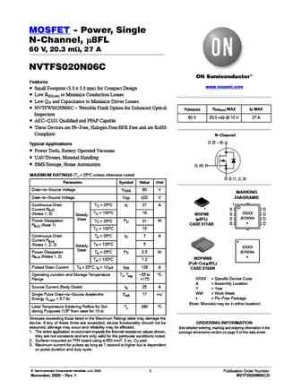
nvtfs020n06c.pdf
MOSFET - Power, Single N-Channel, m8FL 60 V, 20.3 mW, 27 A NVTFS020N06C Features www.onsemi.com Small Footprint (3.3 x 3.3 mm) for Compact Design Low RDS(on) to Minimize Conduction Losses Low QG and Capacitance to Minimize Driver Losses NVTFWS020N06C - Wettable Flank Option for Enhanced Optical V(BR)DSS RDS(on) MAX ID MAX Inspection 60 V 20.3 mW @ 10 V 27 A AEC-
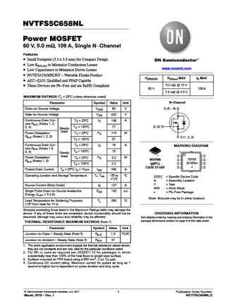
nvtfs5c658nl.pdf
NVTFS5C658NL Power MOSFET 60 V, 5.0 mW, 109 A, Single N-Channel Features Small Footprint (3.3 x 3.3 mm) for Compact Design Low RDS(on) to Minimize Conduction Losses www.onsemi.com Low Capacitance to Minimize Driver Losses NVTFS5C658NLWF - Wettable Flanks Product V(BR)DSS RDS(on) MAX ID MAX AEC-Q101 Qualified and PPAP Capable 5.0 mW @ 10 V These Devices are Pb
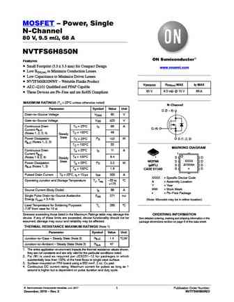
nvtfs6h850n.pdf
MOSFET Power, Single N-Channel 80 V, 9.5 mW, 68 A NVTFS6H850N Features Small Footprint (3.3 x 3.3 mm) for Compact Design www.onsemi.com Low RDS(on) to Minimize Conduction Losses Low Capacitance to Minimize Driver Losses NVTFS6H850NWF - Wettable Flanks Product V(BR)DSS RDS(on) MAX ID MAX AEC-Q101 Qualified and PPAP Capable 80 V 9.5 mW @ 10 V 68 A These De
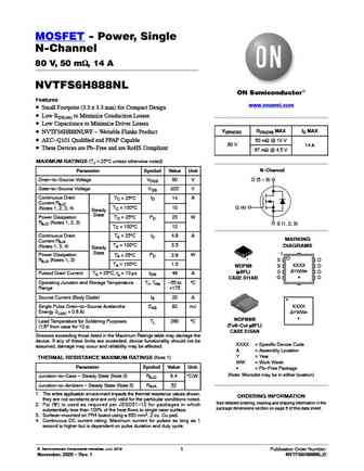
nvtfs6h888nl.pdf
MOSFET - Power, Single N-Channel 80 V, 50 mW, 14 A NVTFS6H888NL Features www.onsemi.com Small Footprint (3.3 x 3.3 mm) for Compact Design Low RDS(on) to Minimize Conduction Losses Low Capacitance to Minimize Driver Losses V(BR)DSS RDS(ON) MAX ID MAX NVTFS6H888NLWF - Wettable Flanks Product AEC-Q101 Qualified and PPAP Capable 50 mW @ 10 V 80 V 14 A These Dev
nvtfs004n04c.pdf
NVTFS004N04C MOSFET Power, Single N-Channel 40 V, 4.9 mW, 77 A Features www.onsemi.com Small Footprint (3.3 x 3.3 mm) for Compact Design Low RDS(on) to Minimize Conduction Losses Low Capacitance to Minimize Driver Losses NVTFWS004N04C - Wettable Flanks Product V(BR)DSS RDS(on) MAX ID MAX AEC-Q101 Qualified and PPAP Capable 40 V 4.9 mW @ 10 V 77 A These De
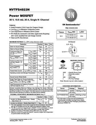
nvtfs4823n-d.pdf
NVTFS4823N Power MOSFET 30 V, 10.5 mW, 30 A, Single N-Channel Features Small Footprint (3.3x3.3 mm) for Compact Design http //onsemi.com Low RDS(on) to Minimize Conduction Losses Low Capacitance to Minimize Driver Losses V(BR)DSS RDS(on) MAX ID MAX NV Prefix for Automotive and Other Applications Requiring 10.5 mW @ 10 V AEC-Q101 Qualified Site and Change Controls 30
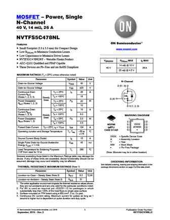
nvtfs5c478nl.pdf
MOSFET Power, Single N-Channel 40 V, 14 mW, 26 A NVTFS5C478NL Features Small Footprint (3.3 x 3.3 mm) for Compact Design www.onsemi.com Low RDS(on) to Minimize Conduction Losses Low Capacitance to Minimize Driver Losses NVTFS5C478NLWF - Wettable Flanks Product V(BR)DSS RDS(on) MAX ID MAX AEC-Q101 Qualified and PPAP Capable 14 mW @ 10 V These Devices are
nvtfs6h888n.pdf
MOSFET - Power, Single N-Channel 80 V, 55 mW, 13 A NVTFS6H888N Features www.onsemi.com Small Footprint (3.3 x 3.3 mm) for Compact Design Low RDS(on) to Minimize Conduction Losses Low Capacitance to Minimize Driver Losses V(BR)DSS RDS(on) MAX ID MAX NVTFS6H888NWF - Wettable Flanks Product AEC-Q101 Qualified and PPAP Capable 80 V 55 mW @ 10 V 13 A These Device
Otros transistores... NVTFS6H854N , NVTFS6H854NL , NVTFS6H860N , NVTFS6H860NL , NVTFS6H880N , NVTFS6H880NL , NVTFS6H888N , NVTFS6H888NL , IRFB4227 , STD25P03L , PJM02N60SA , PJM07P20SA , PJM10H03NSC , PJM138NSA , PJM2300NSA , PJM2300NSA-L , PJM2301PSA .


Liste
Recientemente añadidas las descripciónes de los transistores:
MOSFET: AOT66613L | AOSP21313C | AOSP21311C | AOB66918L | AO3415C | AOTF20N40L | AOTF11N60L | AOT11N60L | AONS21303C | AOI280A60 | AOB66914L | AO3485C | AOI780A70 | AOB42S60L | AOTF950A70L | AOTF27S60L
Popular searches
g40t60an3h datasheet | j5027-r datasheet | transistor a1015 datasheet | bf199 transistor equivalent | bu801 | c8550 transistor datasheet | mj21194 transistor datasheet | kep40n26

