PJM2319PSA MOSFET Equivalente. Reemplazo. Hoja de especificaciones. Principales características
Número de Parte: PJM2319PSA
Tipo de FET: MOSFET
Polaridad de transistor: P
ESPECIFICACIONES MÁXIMAS
Pdⓘ - Máxima disipación de potencia: 1.25 W
|Vds|ⓘ - Voltaje máximo drenador-fuente: 40 V
|Vgs|ⓘ - Voltaje máximo fuente-puerta: 20 V
|Id|ⓘ - Corriente continua de drenaje: 4.4 A
Tjⓘ - Temperatura máxima de unión: 150 °C
CARACTERÍSTICAS ELÉCTRICAS
trⓘ - Tiempo de subida: 9 nS
Cossⓘ - Capacitancia de salida: 76 pF
RDSonⓘ - Resistencia estado encendido drenaje a fuente: 0.08 Ohm
Encapsulados: SOT23
Búsqueda de reemplazo de PJM2319PSA MOSFET
- Selecciónⓘ de transistores por parámetros
PJM2319PSA datasheet
pjm2319psa.pdf
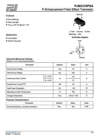
PJM2319PSA P-Enhancement Field Effect Transistor SOT-23 Features Fast Switching Ultra Low Qgd RDS(on) 80 m @V = -10V GS 1. Gate 2.Source 3.Drain Marking S19 Application Schematic Diagram Load Switch Drain DC/DC Converter 3 1 Gate Source 2 Absolute Maximum Ratings Ratings at TA =25 unless otherwise specified. Parameter Symbol Value Unit D
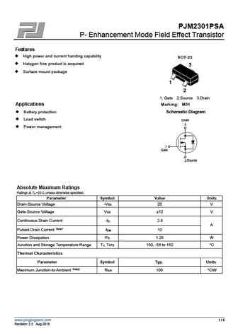
pjm2301psa-s.pdf
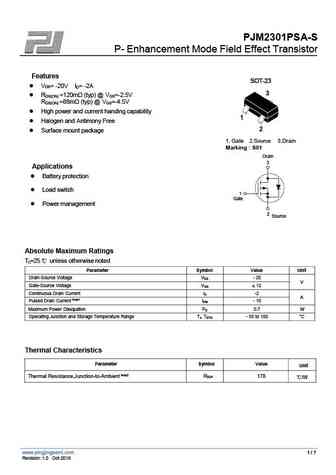
PJM2301PSA-S P- Enhancement Mode Field Effect Transistor Features SOT-23 VDS= -20V I = -2A D R =120m (typ) @ V =-2.5V DS(ON) GS R =88m (typ) @ V =-4.5V DS(ON) GS High power and current handing capability Halogen and Antimony Free Surface mount package 1. Gate 2.Source 3.Drain Marking S01 Drain 3 Applications Battery protection Load s
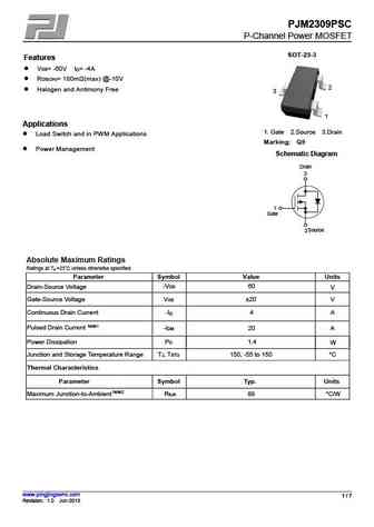
pjm2305psa.pdf
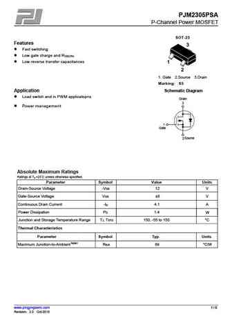
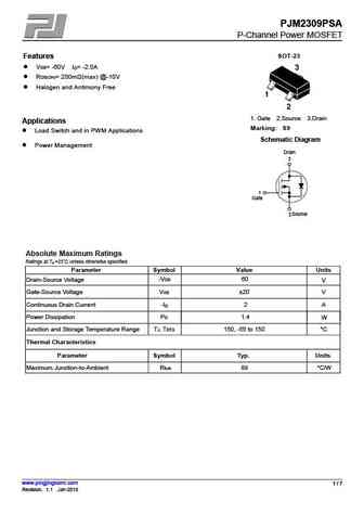
PJM2305PSA P-Channel Power MOSFET SOT-23 Features Fast switching Low gate charge and R DS(ON) Low reverse transfer capacitances 1. Gate 2.Source 3.Drain Marking S5 Application Schematic Diagram Load switch and in PWM applicatopns Drain 3 Power management 1 Gate Source 2 Absolute Maximum Ratings Ratings at TA =25 unless otherwise specified. Paramete
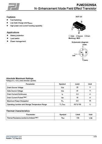
pjm2300nsa-l.pdf
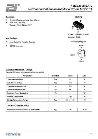
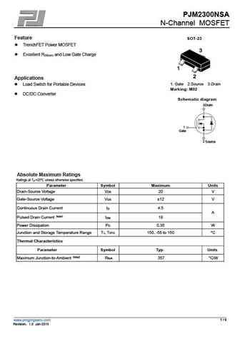
PJM2300NSA-L N-Channel Enhancement Mode Power MOSFET Features SOT-23 Excellent R and Low Gate Charge DS(ON) VDS= 20V I = 5.5A D R
Otros transistores... PJM2300NSA-L , PJM2301PSA , PJM2301PSA-S , PJM2302NSA , PJM2302NSA-S , PJM2305PSA , PJM2309PSA , PJM2309PSC , 2N7002 , PJM3400NSA , PJM3400NSC , PJM3401PSA , PJM3401PSC , PJM3407PSA , PJM3415PSA , PJM84PSA , EM6M2 .
History: SI1028X | HY3810PM | SI6423DQ-T1 | SM4504NHKP | SM1102PSF | ISCNH327P | STD15NF10
History: SI1028X | HY3810PM | SI6423DQ-T1 | SM4504NHKP | SM1102PSF | ISCNH327P | STD15NF10
🌐 : EN ES РУ

Liste
Recientemente añadidas las descripciónes de los transistores:
MOSFET: AUB034N10 | AUB033N08BG | AUB026N085 | AUA062N08BG | AUA060N08AG | AUA056N08BGL | AUA039N10 | ASW80R290E | ASW65R120EFD | ASW65R110E | ASW65R095EFD | ASW65R046EFD | ASW65R041EFDA | ASW65R041E | ASW60R150E | ASW60R090EFDA
Popular searches
irf640n | 2n3904 | bc547 datasheet | k3797 mosfet | bs170 datasheet | tip41c | irfp460 | irfz44n mosfet