SE20075 MOSFET Equivalente. Reemplazo. Hoja de especificaciones. Principales características
Número de Parte: SE20075
Tipo de FET: MOSFET
Polaridad de transistor: N
ESPECIFICACIONES MÁXIMAS
Pdⓘ - Máxima disipación de potencia: 360 W
|Vds|ⓘ - Voltaje máximo drenador-fuente: 200 V
|Vgs|ⓘ - Voltaje máximo fuente-puerta: 20 V
|Id|ⓘ - Corriente continua de drenaje: 75 A
Tjⓘ - Temperatura máxima de unión: 175 °C
CARACTERÍSTICAS ELÉCTRICAS
trⓘ - Tiempo de subida: 18 nS
Cossⓘ - Capacitancia de salida: 950 pF
RDSonⓘ - Resistencia estado encendido drenaje a fuente: 0.018 Ohm
Encapsulados: TO220
Búsqueda de reemplazo de SE20075 MOSFET
- Selecciónⓘ de transistores por parámetros
SE20075 datasheet
se20075.pdf
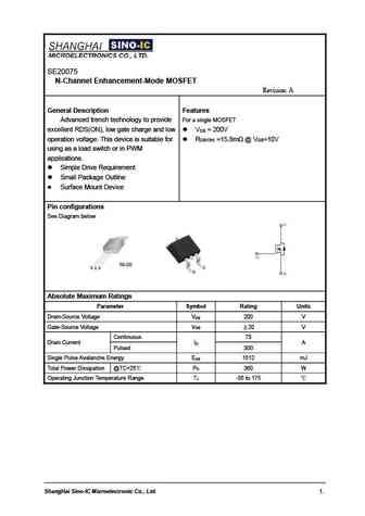
SE20075 N-Channel Enhancement-Mode MOSFET Revision A General Description Features For a single MOSFET Advanced trench technology to provide excellent RDS(ON), low gate charge and low V = 200V DS operation voltage. This device is suitable for R =15.8m @V =10V DS(ON) GS using as a load switch or in PWM applications. Simple Drive Requirement Small Package Outline
kse200.pdf
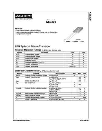
KSE200 Feature Low Collector-Emitter Saturation Voltage High Current Gain Bandwidth Product fT=65MHz @ IC=100mA (Min.) Complement to KSE210 TO-126 1 1. Emitter 2.Collector 3.Base NPN Epitaxial Silicon Transistor Absolute Maximum Ratings TC=25 C unless otherwise noted Symbol Parameter Value Units VCBO Collector-Base Voltage 40 V VCEO Collector-Emitter Voltage 25 V
kse200.pdf
KSE200 POWER TR CD-ROM(Edition.1.1) This Data Sheet is subject to change without notice. (C) 1994 Samsung Electronics Printed in Korea. Page 1 (KSE200) KSE200 POWER TR CD-ROM(Edition.1.1) This Data Sheet is subject to change without notice. (C) 1994 Samsung Electronics Printed in Korea. Page 2 (KSE200)
Otros transistores... SE150180G , SE150180GTS , SE15N50FRA , SE18NS65A , SE1991G , SE1991GA , SE200100G , SE20040 , 18N50 , SE2060 , SE20N110 , SE20P03 , SE2101 , SE2101E , SE2102M , SE2300 , SE2302U .
🌐 : EN ES РУ

Liste
Recientemente añadidas las descripciónes de los transistores:
MOSFET: AUB062N08BG | AUB060N08AG | AUB056N10 | AUB056N08BGL | AUB050N085 | AUB050N055 | AUB045N12 | AUB045N10BT | AUB039N10 | AUB034N10 | AUB033N08BG | AUB026N085 | AUA062N08BG | AUA060N08AG | AUA056N08BGL | AUA039N10
Popular searches
a933 transistor | d209l | irfb4321 | 2n333 | c3852 | irfp140 | ksc2383 datasheet | 2n3906 equivalent