SM4927BSKC MOSFET Equivalente. Reemplazo. Hoja de especificaciones. Principales características
Número de Parte: SM4927BSKC
Tipo de FET: MOSFET
Polaridad de transistor: P
ESPECIFICACIONES MÁXIMAS
Pdⓘ - Máxima
disipación de potencia: 2.5 W
|Vds|ⓘ - Voltaje máximo drenador-fuente: 30 V
|Vgs|ⓘ - Voltaje máximo fuente-puerta: 20 V
|Id|ⓘ - Corriente continua
de drenaje: 8.3 A
Tjⓘ - Temperatura máxima de unión: 150 °C
CARACTERÍSTICAS ELÉCTRICAS
trⓘ - Tiempo
de subida: 8 nS
Cossⓘ - Capacitancia de salida: 215 pF
RDSonⓘ - Resistencia estado encendido drenaje a fuente: 0.021 typ Ohm
Encapsulados: SO8
Búsqueda de reemplazo de SM4927BSKC MOSFET
- Selecciónⓘ de transistores por parámetros
SM4927BSKC datasheet
..1. Size:882K cn vbsemi
sm4927bskc.pdf 
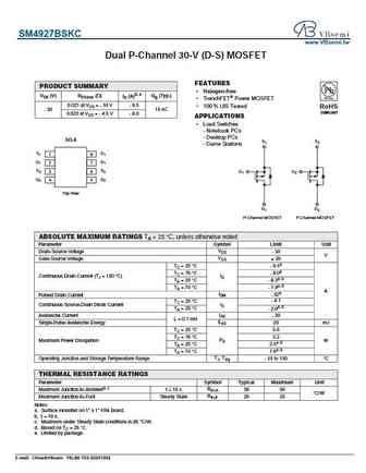
SM4927BSKC www.VBsemi.tw Dual P-Channel 30-V (D-S) MOSFET FEATURES PRODUCT SUMMARY Halogen-free VDS (V) RDS(on) ( ) ID (A)d, e Qg (Typ.) TrenchFET Power MOSFET 0.021 at VGS = - 10 V - 9.5 100 % UIS Tested RoHS - 30 15 nC COMPLIANT 0.028 at VGS = - 4.5 V - 8.0 APPLICATIONS Load Switches - Notebook PCs - Desktop PCs SO-8 S1 S2 - Game Stations S1 1 D1 8
5.1. Size:266K sino
sm4927bsk.pdf 
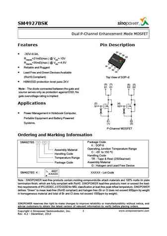
SM4927BSK Dual P-Channel Enhancement Mode MOSFET Features Pin Description D1 D1 -30V/-8.9A, D2 D2 RDS(ON)=21m (max.) @ VGS=-10V RDS(ON)=35m (max.) @ VGS=-4.5V S1 Reliable and Rugged G1 S2 G2 Lead Free and Green Devices Available (RoHS Compliant) Top View of SOP 8 HBM ESD protection level pass 2KV (8) (7) (6) (5) D1 D1 D2 D2 Note The diode connected between the gat
9.1. Size:503K taiwansemi
tsm4925dcs.pdf 
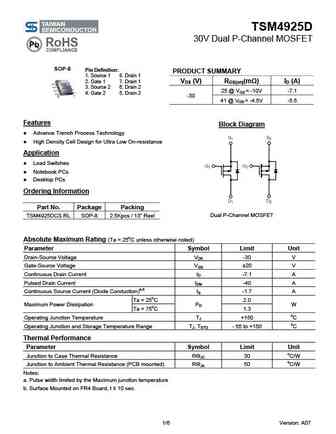
TSM4925D 30V Dual P-Channel MOSFET SOP-8 Pin Definition PRODUCT SUMMARY 1. Source 1 8. Drain 1 2. Gate 1 7. Drain 1 VDS (V) RDS(on)(m ) ID (A) 3. Source 2 6. Drain 2 25 @ VGS = -10V -7.1 4. Gate 2 5. Drain 2 -30 41 @ VGS = -4.5V -5.5 Features Block Diagram Advance Trench Process Technology High Density Cell Design for Ultra Low On-resistance Applicati
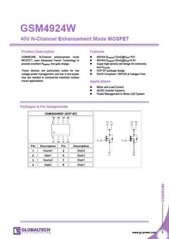
9.2. Size:1468K globaltech semi
gsm4924.pdf 
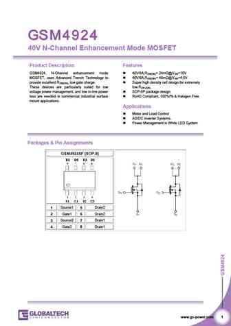
40V N-Channel Enhancement Mode MOSFET Product Description Features GSM4924, N-Channel enhancement mode 40V/8A,RDS(ON)= 24m @VGS=10V MOSFET, uses Advanced Trench Technology to 40V/6A,RDS(ON)= 48m @VGS=4.5V provide excellent RDS(ON), low gate charge. Super high density cell design for extremely These devices are particularly suited for low low RDS (ON) voltage power ma
9.3. Size:834K globaltech semi
gsm4925ws.pdf 
GSM4925WS 30V P-Channel Enhancement Mode MOSFET Product Description Features GSM4925WS, P-Channel enhancement mode -30V/-8.0A,RDS(ON)= 18m @VGS= -10V OSFET, uses Advanced Trench Technology to -30V/-6.0A,RDS(ON)= 26m @VGS= -4.5V provide excellent RDS(ON), low gate charge. Super high density cell design for extremely low RDS (ON) These devices are particularly suite
9.4. Size:719K globaltech semi
gsm4925.pdf 
GSM4925 30V P-Channel Enhancement Mode MOSFET Product Description Features GSM4925, P-Channel enhancement mode -30V/-7.2A,RDS(ON)= 28m @VGS= -10V OSFET, uses Advanced Trench Technology to -30V/-5.8A,RDS(ON)= 37m @VGS= -4.5V provide excellent RDS(ON), low gate charge. Super high density cell design for extremely low RDS (ON) These devices are particularly suited fo
9.5. Size:1478K globaltech semi
gsm4924w.pdf 
GSM4924W 40V N-Channel Enhancement Mode MOSFET Product Description Features GSM4924W, N-Channel enhancement mode 40V/8A,RDS(ON)=22m @VGS=10V MOSFET, uses Advanced Trench Technology to 40V/6A,RDS(ON)=28m @VGS=4.5V provide excellent RDS(ON), low gate charge. Super high density cell design for extremely low RDS (ON) These devices are particularly suited for low S
9.6. Size:833K globaltech semi
gsm4925s.pdf 
GSM4925S 30V P-Channel Enhancement Mode MOSFET Product Description Features GSM4925S, P-Channel enhancement mode -30V/-7.5A,RDS(ON)= 18m @VGS= -10V OSFET, uses Advanced Trench Technology to -30V/-6.0A,RDS(ON)= 26m @VGS= -4.5V provide excellent RDS(ON), low gate charge. Super high density cell design for extremely low RDS (ON) These devices are particularly suited
9.7. Size:823K globaltech semi
gsm4925w.pdf 
GSM4925W 30V P-Channel Enhancement Mode MOSFET Product Description Features GSM4925W, P-Channel enhancement mode -30V/-7.2A,RDS(ON)= 30m @VGS= -10V OSFET, uses Advanced Trench Technology to -30V/-5.8A,RDS(ON)= 36m @VGS= -4.5V provide excellent RDS(ON), low gate charge. Super high density cell design for extremely low RDS (ON) These devices are particularly suited
9.8. Size:846K globaltech semi
gsm4922w.pdf 
GSM4922W 100V N-Channel Enhancement Mode MOSFET Product Description Features GSM4922W, N-Channel enhancement mode 100V/2.0A,RDS(ON)=290m @VGS=10V MOSFET, uses Advanced Trench Technology to 100V/1.5A,RDS(ON)=300m @VGS=4.5V provide excellent RDS(ON), low gate charge. Super high density cell design for extremely low RDS (ON) These devices are particularly suited for
9.9. Size:310K silicon standard
ssm4924gm.pdf 
SSM4924GM Dual N-channel Enhancement-mode Power MOSFETs Simple drive requirement BV BVDSS 20V D2 D2 D1 Lower gate charge R RDS(ON) 35m D1 Fast switching characteristics I 6A ID G2 S2 Pb-free; RoHS compliant. G1 SO-8 S1 DESCRIPTION D2 D1 Advanced Power MOSFETs from Silicon Standard provide the designer with the best combination of fast switching, ruggedized device desig
9.10. Size:153K silicon standard
ssm4920m.pdf 
SSM4920M N-CHANNEL ENHANCEMENT-MODE POWER MOSFET Simple Drive Requirement BV 25V DSS D2 D2 Low On-resistance R 25m D1 DS(ON) D1 Fast Switching I 7A D G2 S2 G1 SO-8 S1 Description D2 D1 Power MOSFETs from Silicon Standard provide the designer with the best combination of fast switching, G2 ruggedized device design, low on-resistance and cost- G1 effectiveness. S1 S2
Otros transistores... SI9955DY
, SIR422DP-T1-GE3
, SIR462DP-T1
, SIR802DP-T1-GE3
, SM2300NSAC
, SM3113NSUC
, SM4028NSUC-TRG
, SM4307PSKPC
, 20N50
, SM4953KC
, SP8K1TB
, SP8M3-TB
, SPD09N05
, SPN2054T252RG
, SPN2302S23R
, SPN3414S23RGB
, SPN4412WS8RG
.