NCE20P45Q MOSFET Equivalente. Reemplazo. Hoja de especificaciones. Principales características
Número de Parte: NCE20P45Q
Tipo de FET: MOSFET
Polaridad de transistor: P
ESPECIFICACIONES MÁXIMAS
Pdⓘ - Máxima disipación de potencia: 80 W
|Vds|ⓘ - Voltaje máximo drenador-fuente: 19 V
|Vgs|ⓘ - Voltaje máximo fuente-puerta: 12 V
|Id|ⓘ - Corriente continua de drenaje: 45 A
Tjⓘ - Temperatura máxima de unión: 150 °C
CARACTERÍSTICAS ELÉCTRICAS
trⓘ - Tiempo de subida: 42 nS
Cossⓘ - Capacitancia de salida: 577 pF
RDSonⓘ - Resistencia estado encendido drenaje a fuente: 0.007 Ohm
Encapsulados: DFN3.3X3.3EP
Búsqueda de reemplazo de NCE20P45Q MOSFET
- Selecciónⓘ de transistores por parámetros
NCE20P45Q datasheet
nce20p45q.pdf
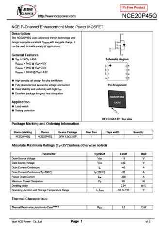
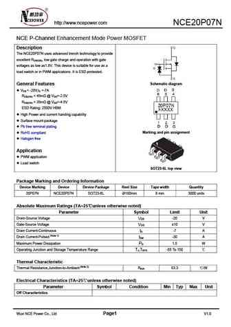
Pb Free Product http //www.ncepower.com NCE20P45Q NCE P-Channel Enhancement Mode Power MOSFET Description The NCE20P45Q uses advanced trench technology and design to provide excellent RDS(ON) with low gate charge. It can be used in a wide variety of applications. General Features VDS =-19V,ID =-45A Schematic diagram RDS(ON)
nce20p05y.pdf
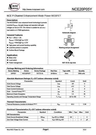
http //www.ncepower.com NCE20P05Y NCE P-Channel Enhancement Mode Power MOSFET Description The NCE20P05Y uses advanced trench technology to provide excellent R , low gate charge and operation with gate DS(ON) voltages as low as 2.5V. This device is suitable for use as a load switch or in PWM applications. Schematic diagram General Features V = -20V,I = -5A DS D R
nce20pd05.pdf
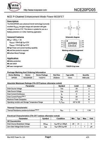
http //www.ncepower.com NCE20PD05 NCE P-Channel Enhancement Mode Power MOSFET Description The NCE20PD05 uses advanced trench technology to provide excellent RDS(ON), low gate charge and operation with gate voltages as low as 2.5V. This device is suitable for use as a Battery protection or in other Switching application. Schematic diagram General Features VDS = -20V,ID =- 5
nce20p10j.pdf
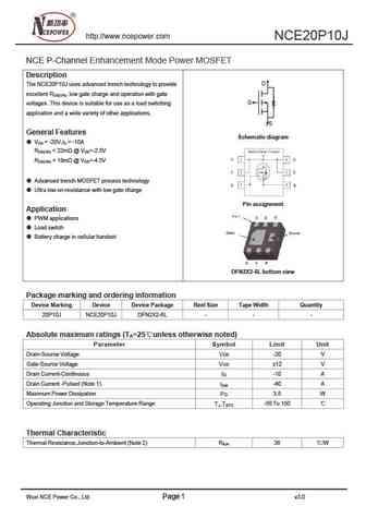
http //www.ncepower.com NCE20P10J NCE P-Channel Enhancement Mode Power MOSFET Description D The NCE20P10J uses advanced trench technology to provide excellent R , low gate charge and operation with gate DS(ON) G voltages .This device is suitable for use as a load switching application and a wide variety of other applications. S General Features Schematic diagram V = -20V,I = -

Otros transistores... NCE1550, NCE1570, NCE2003, NCE2007N, NCE2010E, NCE2030, NCE2030K, NCE2060K, CS150N03A8, NCE20P70G, NCE2301, NCE2302, NCE2303, NCE2304, NCE2305, NCE2309, NCE2312
History: IXTH02N450HV
🌐 : EN ES РУ

Liste
Recientemente añadidas las descripciónes de los transistores:
MOSFET: AKF30N5P0SX | AKF30N10S | AKF20P45D | CM4407 | CM3407 | CM3400 | SVF11N65F | SVF11N65T | FKBB3105 | EHBA036R1 | CRTT067N10N | AP6NA3R2MT | AP65SA145DDT8 | AP4NAR95CMT-A | AP4024GEMT-HF | AP3P050AH
Popular searches
20n50 | 2sc869 | tip29 transistor equivalent | 2n555 | 2sa564a | c815 transistor | ksa1381 equivalent | 2sa1306