NCE20P45Q Specs and Replacement
Type Designator: NCE20P45Q
Type of Transistor: MOSFET
Type of Control Channel: P-Channel
Absolute Maximum Ratings
Pd ⓘ - Maximum Power Dissipation: 80 W
|Vds|ⓘ - Maximum Drain-Source Voltage: 19 V
|Vgs|ⓘ - Maximum Gate-Source Voltage: 12 V
|Id| ⓘ - Maximum Drain Current: 45 A
Tj ⓘ - Maximum Junction Temperature: 150 °C
Electrical Characteristics
tr ⓘ - Rise Time: 42 nS
Cossⓘ - Output Capacitance: 577 pF
RDSonⓘ - Maximum Drain-Source On-State Resistance: 0.007 Ohm
Package: DFN3.3X3.3EP
NCE20P45Q substitution
- MOSFET ⓘ Cross-Reference Search
NCE20P45Q datasheet
nce20p45q.pdf
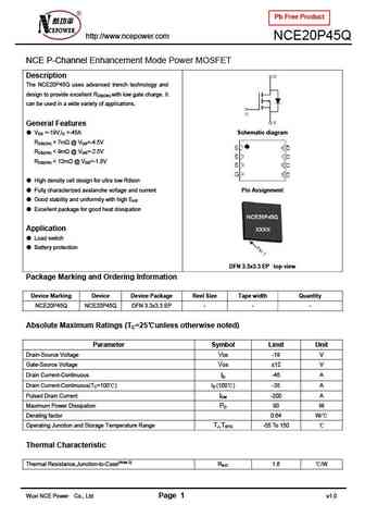
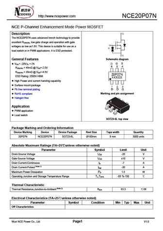
Pb Free Product http //www.ncepower.com NCE20P45Q NCE P-Channel Enhancement Mode Power MOSFET Description The NCE20P45Q uses advanced trench technology and design to provide excellent RDS(ON) with low gate charge. It can be used in a wide variety of applications. General Features VDS =-19V,ID =-45A Schematic diagram RDS(ON) ... See More ⇒
nce20p05y.pdf
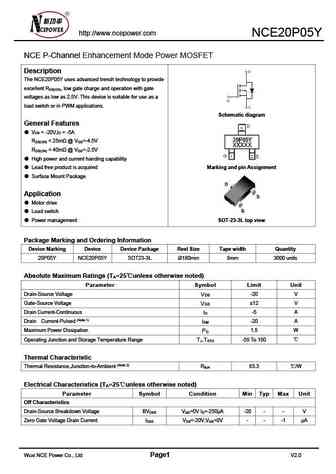
http //www.ncepower.com NCE20P05Y NCE P-Channel Enhancement Mode Power MOSFET Description The NCE20P05Y uses advanced trench technology to provide excellent R , low gate charge and operation with gate DS(ON) voltages as low as 2.5V. This device is suitable for use as a load switch or in PWM applications. Schematic diagram General Features V = -20V,I = -5A DS D R ... See More ⇒
nce20pd05.pdf
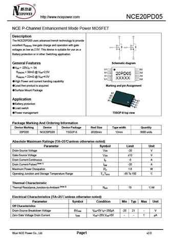
http //www.ncepower.com NCE20PD05 NCE P-Channel Enhancement Mode Power MOSFET Description The NCE20PD05 uses advanced trench technology to provide excellent RDS(ON), low gate charge and operation with gate voltages as low as 2.5V. This device is suitable for use as a Battery protection or in other Switching application. Schematic diagram General Features VDS = -20V,ID =- 5... See More ⇒
nce20p10j.pdf
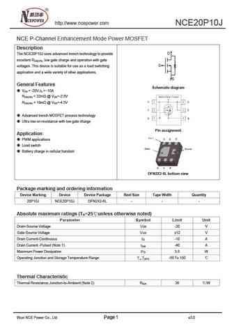
http //www.ncepower.com NCE20P10J NCE P-Channel Enhancement Mode Power MOSFET Description D The NCE20P10J uses advanced trench technology to provide excellent R , low gate charge and operation with gate DS(ON) G voltages .This device is suitable for use as a load switching application and a wide variety of other applications. S General Features Schematic diagram V = -20V,I = -... See More ⇒

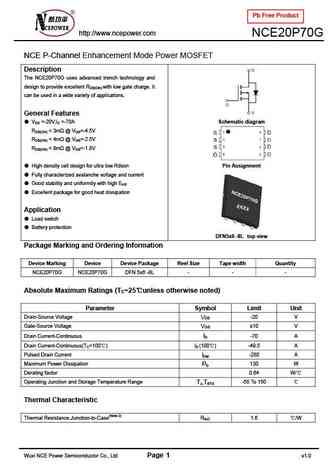
Detailed specifications: NCE1550, NCE1570, NCE2003, NCE2007N, NCE2010E, NCE2030, NCE2030K, NCE2060K, CS150N03A8, NCE20P70G, NCE2301, NCE2302, NCE2303, NCE2304, NCE2305, NCE2309, NCE2312
Keywords - NCE20P45Q MOSFET specs
NCE20P45Q cross reference
NCE20P45Q equivalent finder
NCE20P45Q pdf lookup
NCE20P45Q substitution
NCE20P45Q replacement
Step-by-step guide to finding a MOSFET replacement. Cross-reference parts and ensure compatibility for your repair or project.
