NCE3407 MOSFET Equivalente. Reemplazo. Hoja de especificaciones. Principales características
Número de Parte: NCE3407
Tipo de FET: MOSFET
Polaridad de transistor: P
ESPECIFICACIONES MÁXIMAS
Pdⓘ - Máxima disipación de potencia: 1.4 W
|Vds|ⓘ - Voltaje máximo drenador-fuente: 30 V
|Vgs|ⓘ - Voltaje máximo fuente-puerta: 20 V
|Id|ⓘ - Corriente continua de drenaje: 4.1 A
Tjⓘ - Temperatura máxima de unión: 150 °C
CARACTERÍSTICAS ELÉCTRICAS
trⓘ - Tiempo de subida: 4.5 nS
Cossⓘ - Capacitancia de salida: 105 pF
RDSonⓘ - Resistencia estado encendido drenaje a fuente: 0.065 Ohm
Encapsulados: SOT23
Búsqueda de reemplazo de NCE3407 MOSFET
- Selecciónⓘ de transistores por parámetros
NCE3407 datasheet
nce3407.pdf
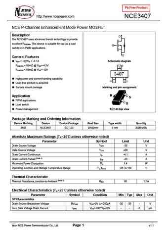
Pb Free Product http //www.ncepower.com NCE3407 NCE P-Channel Enhancement Mode Power MOSFET Description D The NCE3407 uses advanced trench technology to provide excellent RDS(ON), This device is suitable for use as a load G switch or in PWM applications. S General Features VDS = -30V,ID = -4.1A Schematic diagram RDS(ON)
nce3407a.pdf
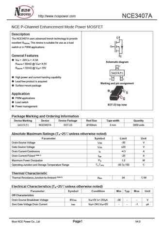
http //www.ncepower.com NCE3407A NCE P-Channel Enhancement Mode Power MOSFET Description D The NCE3407A uses advanced trench technology to provide excellent R , This device is suitable for use as a load DS(ON) G switch or in PWM applications. General Features S V = -30V,I = -4.3A DS D Schematic diagram R
nce3407ay.pdf
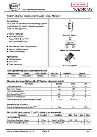
Pb Free Product http //www.ncepower.com NCE3407AY NCE P-Channel Enhancement Mode Power MOSFET D Description The NCE3407AY uses advanced trench technology to provide G excellent RDS(ON), This device is suitable for use as a load switch or in PWM applications. S General Features Schematic diagram VDS = -30V,ID = -4.3A RDS(ON)
nce3407e.pdf
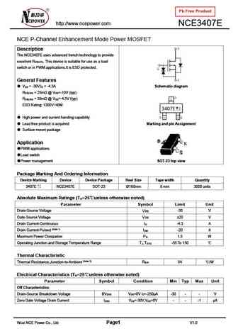
Pb Free Product http //www.ncepower.com NCE3407E NCE P-Channel Enhancement Mode Power MOSFET Description The NCE3407E uses advanced trench technology to provide excellent R . This device is suitable for use as a load DS(ON) switch or in PWM applications.It is ESD protected. General Features V = -30V,I = -4.3A Schematic diagram DS D R = 28m @ V =-10V (typ) DS(ON) GS R = 38m
Otros transistores... NCE30P30K, NCE30P50G, NCE3400, NCE3400AY, NCE3400X, NCE3401, NCE3404Y, NCE3406N, IRF540, NCE3407AY, NCE3415, NCE3416, NCE3420, NCE4009S, NCE4012S, NCE4060I, NCE4060K
History: NCE50NF180I | NCE50NF180K
🌐 : EN ES РУ

Liste
Recientemente añadidas las descripciónes de los transistores:
MOSFET: AKF30N5P0SX | AKF30N10S | AKF20P45D | CM4407 | CM3407 | CM3400 | SVF11N65F | SVF11N65T | FKBB3105 | EHBA036R1 | CRTT067N10N | AP6NA3R2MT | AP65SA145DDT8 | AP4NAR95CMT-A | AP4024GEMT-HF | AP3P050AH
Popular searches
2sc4834 | 2sd313 transistor equivalent | 2sc871 replacement | a872 transistor | b1560 | 2sa1695 | a1175 transistor | 2sc1678