NCE55P15I MOSFET Equivalente. Reemplazo. Hoja de especificaciones. Principales características
Número de Parte: NCE55P15I
Tipo de FET: MOSFET
Polaridad de transistor: P
ESPECIFICACIONES MÁXIMAS
Pdⓘ - Máxima disipación de potencia: 35 W
|Vds|ⓘ - Voltaje máximo drenador-fuente: 55 V
|Vgs|ⓘ - Voltaje máximo fuente-puerta: 20 V
|Id|ⓘ - Corriente continua de drenaje: 15 A
Tjⓘ - Temperatura máxima de unión: 175 °C
CARACTERÍSTICAS ELÉCTRICAS
trⓘ - Tiempo de subida: 9 nS
Cossⓘ - Capacitancia de salida: 145 pF
RDSonⓘ - Resistencia estado encendido drenaje a fuente: 0.075 Ohm
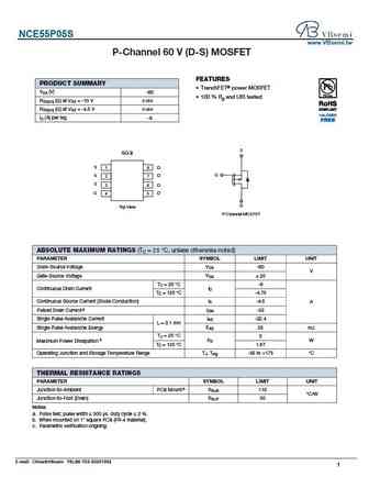
Encapsulados: TO251
Búsqueda de reemplazo de NCE55P15I MOSFET
- Selecciónⓘ de transistores por parámetros
NCE55P15I datasheet
nce55p15i.pdf
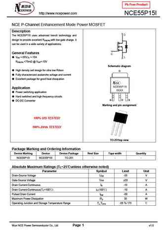
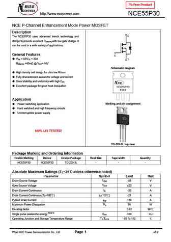
Pb Free Product http //www.ncepower.com NCE55P15I NCE P-Channel Enhancement Mode Power MOSFET Description The NCE55P15I uses advanced trench technology and design to provide excellent RDS(ON) with low gate charge. It can be used in a wide variety of applications. General Features VDS =-55V,ID =-15A RDS(ON)
nce55p15.pdf
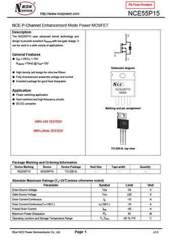
Pb Free Product http //www.ncepower.com NCE55P15 NCE P-Channel Enhancement Mode Power MOSFET Description The NCE55P15 uses advanced trench technology and design to provide excellent RDS(ON) with low gate charge. It can be used in a wide variety of applications. General Features VDS =-55V,ID =-15A RDS(ON)
nce55p15k.pdf
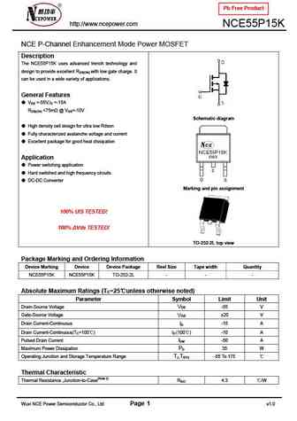
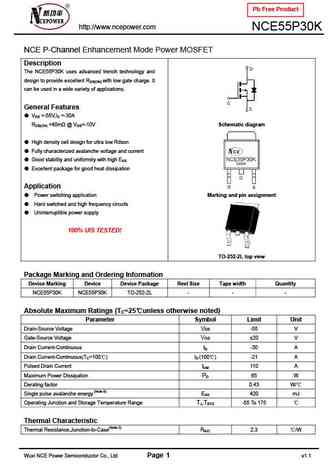
Pb Free Product http //www.ncepower.com NCE55P15K NCE P-Channel Enhancement Mode Power MOSFET Description The NCE55P15K uses advanced trench technology and design to provide excellent RDS(ON) with low gate charge. It can be used in a wide variety of applications. General Features VDS =-55V,ID =-15A RDS(ON)
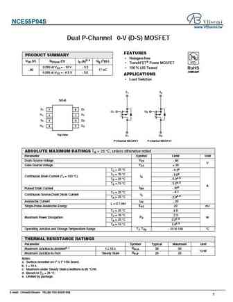
nce55p04s.pdf
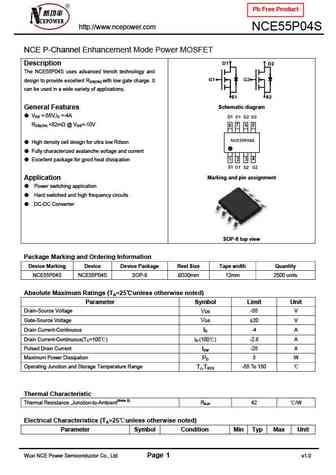
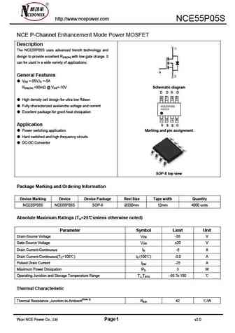
Pb Free Product http //www.ncepower.com NCE55P04S NCE P-Channel Enhancement Mode Power MOSFET Description D1 D2 The NCE55P04S uses advanced trench technology and G1 G2 design to provide excellent RDS(ON) with low gate charge. It can be used in a wide variety of applications. S1 S2 Schematic diagram General Features VDS =-55V,ID =-4A RDS(ON)
Otros transistores... NCE40P40L, NCE40P70K, NCE4435, NCE4606A, NCE4614, NCE4801, NCE4963, NCE55H12, IRFP260, NCE55P15K, NCE55P30, NCE55P30K, NCE6003, NCE6003M, NCE6003Y, NCE6005AR, NCE6008AS
🌐 : EN ES РУ

Liste
Recientemente añadidas las descripciónes de los transistores:
MOSFET: AKF30N5P0SX | AKF30N10S | AKF20P45D | CM4407 | CM3407 | CM3400 | SVF11N65F | SVF11N65T | FKBB3105 | EHBA036R1 | CRTT067N10N | AP6NA3R2MT | AP65SA145DDT8 | AP4NAR95CMT-A | AP4024GEMT-HF | AP3P050AH
Popular searches
2sc2291 | bc139 | 2sc1398 | 2sd218 | bc547 характеристики | me15n10-g | 2n2905 equivalent | 2sa640