HM4887 MOSFET Equivalente. Reemplazo. Hoja de especificaciones. Principales características
Número de Parte: HM4887
Tipo de FET: MOSFET
Polaridad de transistor: P
ESPECIFICACIONES MÁXIMAS
Pdⓘ - Máxima disipación de potencia: 3 W
|Vds|ⓘ - Voltaje máximo drenador-fuente: 100 V
|Vgs|ⓘ - Voltaje máximo fuente-puerta: 20 V
|Id|ⓘ - Corriente continua de drenaje: 4.5 A
Tjⓘ - Temperatura máxima de unión: 150 °C
CARACTERÍSTICAS ELÉCTRICAS
trⓘ - Tiempo de subida: 73 nS
Cossⓘ - Capacitancia de salida: 590 pF
RDSonⓘ - Resistencia estado encendido drenaje a fuente: 0.1 Ohm
Encapsulados: SOP8
Búsqueda de reemplazo de HM4887 MOSFET
- Selecciónⓘ de transistores por parámetros
HM4887 datasheet
hm4887.pdf
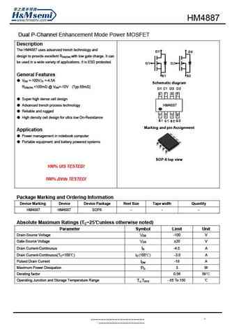
HM4887 Dual P-Channel Enhancement Mode Power MOSFET Description The HM4887 uses advanced trench technology and D1 D2 design to provide excellent RDS(ON) with low gate charge. It can be used in a wide variety of applications. It is ESD protested. G1 G2 General Features S1 S2 VDS =-100V,ID =-4.5A Schematic diagram RDS(ON)
hm4885.pdf
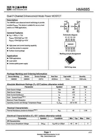
HM4885 Dual P-Channel Enhancement Mode Power MOSFET Description D1 D2 The HM4885 uses advanced trench technology to provide excellent RDS(ON), This device is suitable for use as a load G1 G2 switch or in PWM applications. S1 S2 General Features Schematic diagram VDS = -40V,ID = -7.5A RDS(ON)
hm4884.pdf
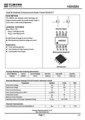
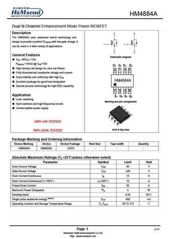
HM Dual N-Channel Enhancement Mode Power MOSFET DESCRIPTION The HM uses advanced trench technology and design to provide excellent RDS(ON) with low gate charge. It can be used in a wide variety of applications. GENERAL FEATURES Schematic diagram VDS =40V,ID =10A RDS(ON)
hm4885a.pdf
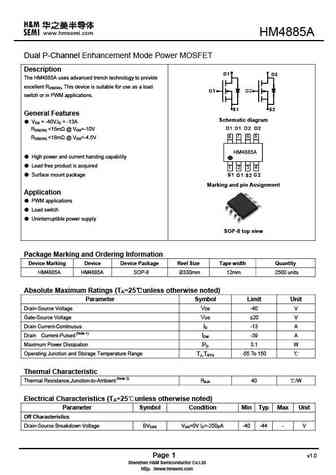
HM4885A Dual P-Channel Enhancement Mode Power MOSFET Description D1 D2 The HM4885A uses advanced trench technology to provide excellent RDS(ON), This device is suitable for use as a load G1 G2 switch or in PWM applications. S1 S2 General Features Schematic diagram VDS = -40V,ID = -13A RDS(ON)
Otros transistores... HM4853A , HM4853B , HM4884 , HM4884A , HM4885 , HM4885A , HM4886A , HM4886E , IRFZ44N , HM4892A , HM4892B , HM4922 , HM4953 , HM4953A , HM4953B , HM4953C , HM4953D .
History: UPA2379T1P
History: UPA2379T1P
🌐 : EN ES РУ

Liste
Recientemente añadidas las descripciónes de los transistores:
MOSFET: AUN084N10 | AUN065N10 | AUN063N10 | AUN062N08BG | AUN060N08AG | AUN053N10 | AUN050N08BGL | AUN045N085 | AUN042N055 | AUN036N10 | AUD069N10A | AUD062N08BG | AUD060N08AG | AUD060N055 | AUD056N08BGL | AUB062N08BG
Popular searches
13003 transistor datasheet | 2n3416 | bdx53c | k3563 | d882p | 2sb1560 | 2n1304 | 2sa979