HM4953 MOSFET Equivalente. Reemplazo. Hoja de especificaciones. Principales características
Número de Parte: HM4953
Tipo de FET: MOSFET
Polaridad de transistor: P
ESPECIFICACIONES MÁXIMAS
Pdⓘ - Máxima disipación de potencia: 2.5 W
|Vds|ⓘ - Voltaje máximo drenador-fuente: 30 V
|Vgs|ⓘ - Voltaje máximo fuente-puerta: 20 V
|Id|ⓘ - Corriente continua de drenaje: 5.1 A
Tjⓘ - Temperatura máxima de unión: 150 °C
CARACTERÍSTICAS ELÉCTRICAS
trⓘ - Tiempo de subida: 13 nS
Cossⓘ - Capacitancia de salida: 420 pF
RDSonⓘ - Resistencia estado encendido drenaje a fuente: 0.055 Ohm
Encapsulados: SOP8
Búsqueda de reemplazo de HM4953 MOSFET
- Selecciónⓘ de transistores por parámetros
HM4953 datasheet
hm4953.pdf

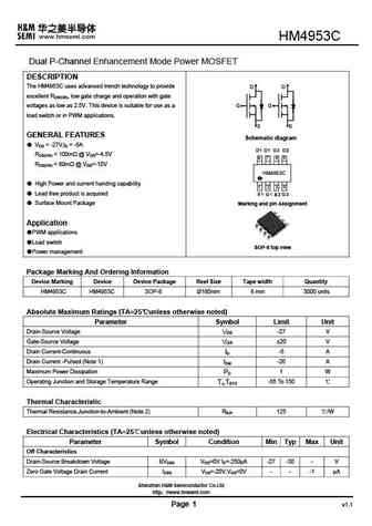
HM4953 Dual P-Channel Enhancement Mode Power MOSFET DESCRIPTION D1 D2 The HM4953 uses advanced trench technology to provide excellent RDS(ON), low gate charge and operation with gate G1 G2 voltages as low as 4.5V. This device is suitable for use as a load switch or in PWM applications. S1 S2 Schematic diagram GENERAL FEATURES VDS = -30V,ID = -5.1A RDS(ON)
chm4953jgp.pdf
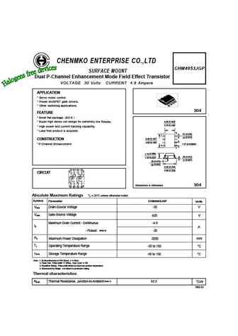
CHENMKO ENTERPRISE CO.,LTD CHM4953JGP SURFACE MOUNT Dual P-Channel Enhancement Mode Field Effect Transistor VOLTAGE 30 Volts CURRENT 4.9 Ampere APPLICATION * Servo motor control. * Power MOSFET gate drivers. * Other switching applications. SO-8 FEATURE * Small flat package. (SO-8 ) ( ) * Super high dense cell design for extremely low RDS(ON). 4.06 0.160 ( ) 3.70 0.146 * High
hm4953c.pdf
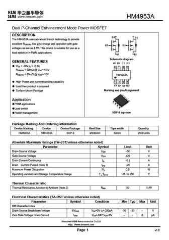
HM4953C Dual P-Channel Enhancement Mode Power MOSFET DESCRIPTION The HM4953C uses advanced trench technology to provide D D excellent RDS(ON), low gate charge and operation with gate voltages as low as 2.5V. This device is suitable for use as a G G load switch or in PWM applications. S S GENERAL FEATURES Schematic diagram VDS = -27V,ID = -5A RDS(ON)
hm4953b.pdf

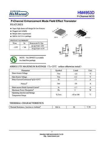
HM4953B Dual P-Channel Enhancement Mode Power MOSFET DESCRIPTION The HM4953B uses advanced trench technology to provide D D excellent RDS(ON), low gate charge and operation with gate voltages as low as 2.5V. This device is suitable for use as a G G load switch or in PWM applications. S S GENERAL FEATURES Schematic diagram VDS = -20V,ID = -5A RDS(ON)
Otros transistores... HM4885 , HM4885A , HM4886A , HM4886E , HM4887 , HM4892A , HM4892B , HM4922 , 20N60 , HM4953A , HM4953B , HM4953C , HM4953D , HM4963 , HM4N10PR , HM4N150T , HM4N60 .
🌐 : EN ES РУ

Liste
Recientemente añadidas las descripciónes de los transistores:
MOSFET: AUN084N10 | AUN065N10 | AUN063N10 | AUN062N08BG | AUN060N08AG | AUN053N10 | AUN050N08BGL | AUN045N085 | AUN042N055 | AUN036N10 | AUD069N10A | AUD062N08BG | AUD060N08AG | AUD060N055 | AUD056N08BGL | AUB062N08BG
Popular searches
d882p | 2sb1560 | 2n1304 | 2sa979 | 2sc4793 | d965 | mje15031 | irfp150n