ASDM30N55E-R MOSFET Equivalente. Reemplazo. Hoja de especificaciones. Principales características
Número de Parte: ASDM30N55E-R
Tipo de FET: MOSFET
Polaridad de transistor: N
ESPECIFICACIONES MÁXIMAS
Pdⓘ - Máxima disipación de potencia: 40 W
|Vds|ⓘ - Voltaje máximo drenador-fuente: 30 V
|Vgs|ⓘ - Voltaje máximo fuente-puerta: 20 V
|Id|ⓘ - Corriente continua de drenaje: 55 A
Tjⓘ - Temperatura máxima de unión: 150 °C
CARACTERÍSTICAS ELÉCTRICAS
trⓘ - Tiempo de subida: 49 nS
Cossⓘ - Capacitancia de salida: 410 pF
RDSonⓘ - Resistencia estado encendido drenaje a fuente: 0.006 Ohm
Encapsulados: DFN3.3X3.3-8L
Búsqueda de reemplazo de ASDM30N55E-R MOSFET
- Selecciónⓘ de transistores por parámetros
ASDM30N55E-R datasheet
asdm30n55e-r.pdf
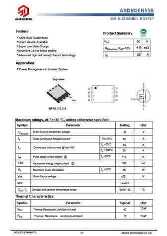
ASDM30N55E 30V N-CHANNEL MOSFET Feature Product Summary 100% EAS Guaranteed VDS 30 V Green Device Available Super Low Gate Charge RDS(on),typ VGS=10V 4.8 m Excellent CdV/dt effect decline A 55 ID Advanced high cell density Trench technology Application Power Management in Inverter System top view DFN3.3*3.3-8 Maximum ratings, at T A=25 C, unless othe
asdm30n55e.pdf

ASDM30N55E 30V N-CHANNEL MOSFET Feature Product Summary 100% EAS Guaranteed VDS 30 V Green Device Available Super Low Gate Charge RDS(on),typ VGS=10V 4.8 m Excellent CdV/dt effect decline A 55 ID Advanced high cell density Trench technology Application Power Management in Inverter System top view DFN3.3*3.3-8 Maximum ratings, at T A=25 C, unless othe
asdm30n65e-r.pdf

ASDM30N65E 30V N-CHANNEL MOSFET Product Summary Feature l Low Gate Charge VDS 30 V l Green Device Available 4.5 m RDS(on),typ VGS=10V l Super Low Gate Charge A 65 ID l Excellent CdV/dt effect decline l Advanced high cell density Trench technology Applications l Power Management in Desktop Computer or DC/DC Converters. l Isolated DC/DC Converters in Telecom and Industrial.
asdm30n65e.pdf
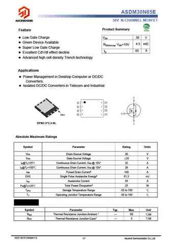
ASDM30N65E 30V N-CHANNEL MOSFET Product Summary Feature l Low Gate Charge VDS 30 V l Green Device Available 4.5 m RDS(on),typ VGS=10V l Super Low Gate Charge A 65 ID l Excellent CdV/dt effect decline l Advanced high cell density Trench technology Applications l Power Management in Desktop Computer or DC/DC Converters. l Isolated DC/DC Converters in Telecom and Industrial.
Otros transistores... AP68N06G , AP80N04G , AP80N04Q , AP90N03Q , AP90P03G , AP90P03Q , APG077N01G , APG095N01G , IRF1404 , ASDM30N65E-R , ASDM30P11TD-R , ASDM30P30CTD-R , ASDM40N52E-R , AUIRFN8405TR , CJAC100SN08U , CJAC110SN10A , CJAC80SN10 .
History: TPCP8305 | WMJ25N70EM | CJBE5005 | 20N03 | NTMS4177PR
History: TPCP8305 | WMJ25N70EM | CJBE5005 | 20N03 | NTMS4177PR
🌐 : EN ES РУ

Liste
Recientemente añadidas las descripciónes de los transistores:
MOSFET: ASU70R600E | ASU65R850E | ASU65R550E | ASU65R350E | ASR65R120EFD | ASR65R046EFD | ASQ65R046EFD | ASM65R280E | ASM60R330E | ASE70R950E | ASD80R750E | ASD70R950E | ASD70R600E | ASD70R380E | ASD65R850E | ASD65R550E
Popular searches
bc109c | d331 transistor | irfbc40 | mp16b transistor | 2sa934 | 2sd118 | 2n3403 | 2sa750