NTMFS015N10MCLT1G MOSFET Equivalente. Reemplazo. Hoja de especificaciones. Principales características
Número de Parte: NTMFS015N10MCLT1G
Tipo de FET: MOSFET
Polaridad de transistor: N
ESPECIFICACIONES MÁXIMAS
Pdⓘ - Máxima
disipación de potencia: 79 W
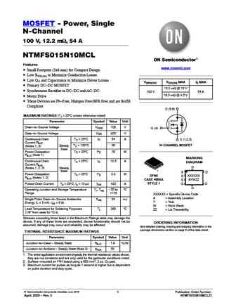
|Vds|ⓘ - Voltaje máximo drenador-fuente: 100 V
|Vgs|ⓘ - Voltaje máximo fuente-puerta: 20 V
|Id|ⓘ - Corriente continua
de drenaje: 54 A
Tjⓘ - Temperatura máxima de unión: 175 °C
CARACTERÍSTICAS ELÉCTRICAS
trⓘ - Tiempo
de subida: 10 nS
Cossⓘ - Capacitancia de salida: 521 pF
RDSonⓘ - Resistencia estado encendido drenaje a fuente: 0.0122 Ohm
Encapsulados: DFN5
Búsqueda de reemplazo de NTMFS015N10MCLT1G MOSFET
- Selecciónⓘ de transistores por parámetros
NTMFS015N10MCLT1G datasheet
7.1. Size:137K onsemi
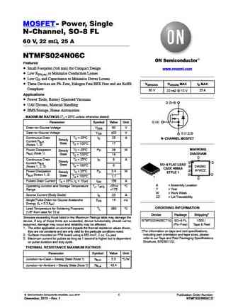
ntmfs016n06c.pdf 
MOSFET- Power, Single N-Channel, SO-8FL 60 V, 15.6 mW, 33 A NTMFS016N06C Features Small Footprint (5x6 mm) for Compact Design www.onsemi.com Low RDS(on) to Minimize Conduction Losses Low QG and Capacitance to Minimize Driver Losses These Devices are Pb-Free, Halogen Free/BFR Free and are RoHS V(BR)DSS RDS(ON) MAX ID MAX Compliant 60 V 15.6 mW @ 10 V 33 A Applications
8.1. Size:187K 1
ntmfs0d8n02p1et1g.pdf

MOSFET - Power, Single N-Channel, SO8-FL 25 V, 0.68 mW, 365 A NTMFS0D8N02P1E Features Small Footprint (5x6mm) for Compact Design www.onsemi.com Low RDS(on) to Minimize Conduction Losses Low QG and Capacitance to Minimize Driver Losses These Devices are Pb-Free, Halogen Free/BFR Free and are RoHS V(BR)DSS RDS(ON) MAX ID MAX Compliant 0.68 mW @ 10 V 25 V 365 A Applic
8.2. Size:176K 1
ntmfs0d9n03cgt1g.pdf

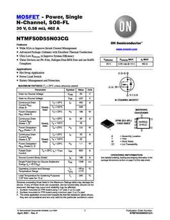
MOSFET - Power, Single N-Channel, SO8-FL 30 V, 0.9 mW, 298 A NTMFS0D9N03CG Features www.onsemi.com Advanced Package (5x6mm) with Excellent Thermal Conduction Ultra Low RDS(on) to Improve System Efficiency These Devices are Pb-Free, Halogen Free/BFR Free and are RoHS V(BR)DSS RDS(ON) MAX ID MAX Compliant 30 V 0.9 mW @ 10 V 298 A Applications Hot Swap Application D (
8.3. Size:185K 1
ntmfs006n12mct1g.pdf
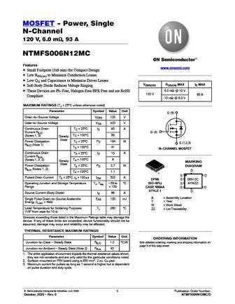
MOSFET - Power, Single N-Channel 120 V, 6.0 mW, 93 A NTMFS006N12MC Features www.onsemi.com Small Footprint (5x6 mm) for Compact Design Low RDS(on) to Minimize Conduction Losses Low QG and Capacitance to Minimize Driver Losses V(BR)DSS RDS(ON) MAX ID MAX Soft Body Diode Reduces Voltage Ringing 6.0 mW @ 10 V These Devices are Pb-Free, Halogen Free/BFR Free and are
8.4. Size:200K 1
ntmfs008n12mct1g.pdf

ON Semiconductor Is Now To learn more about onsemi , please visit our website at www.onsemi.com onsemi and and other names, marks, and brands are registered and/or common law trademarks of Semiconductor Components Industries, LLC dba onsemi or its affiliates and/or subsidiaries in the United States and/or other countries. onsemi owns the rights to a number of patents, trademarks,
8.5. Size:178K onsemi
ntmfs020n06c.pdf

MOSFET- Power, Single N-Channel, SO8FL 60 V, 19.6 mW, 28 A NTMFS020N06C Features Small Footprint (5x6 mm) for Compact Design www.onsemi.com Low RDS(on) to Minimize Conduction Losses Low QG and Capacitance to Minimize Driver Losses These Devices are Pb-Free, Halogen Free/BFR Free and are RoHS V(BR)DSS RDS(ON) MAX ID MAX Compliant 60 V 19.6 mW @ 10 V 28 A Applications
8.6. Size:187K onsemi
ntmfs0d8n02p1e.pdf
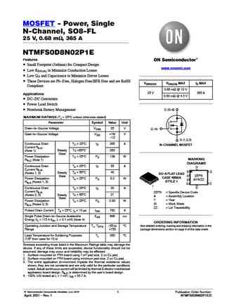
MOSFET - Power, Single N-Channel, SO8-FL 25 V, 0.68 mW, 365 A NTMFS0D8N02P1E Features Small Footprint (5x6mm) for Compact Design www.onsemi.com Low RDS(on) to Minimize Conduction Losses Low QG and Capacitance to Minimize Driver Losses These Devices are Pb-Free, Halogen Free/BFR Free and are RoHS V(BR)DSS RDS(ON) MAX ID MAX Compliant 0.68 mW @ 10 V 25 V 365 A Applic
8.7. Size:169K onsemi
ntmfs0d55n03cg.pdf
MOSFET - Power, Single N-Channel, SO8-FL 30 V, 0.58 mW, 462 A NTMFS0D55N03CG Features Wide SOA to Improve Inrush Current Management www.onsemi.com Advanced Package (5x6mm) with Excellent Thermal Conduction Ultra Low RDS(on) to Improve System Efficiency V(BR)DSS RDS(ON) MAX ID MAX These Devices are Pb-Free, Halogen Free/BFR Free and are RoHS Compliant 30 V 0.58 mW @ 1
8.8. Size:1406K onsemi
ntmfs08n003c.pdf
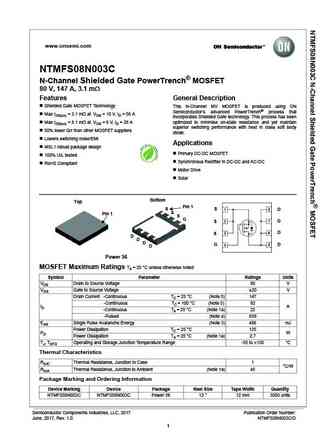
www.onsemi.com NTMFS08N003C N-Channel Shielded Gate PowerTrench MOSFET 80 V, 147 A, 3.1 m Features General Description Shielded Gate MOSFET Technology This N-Channel MV MOSFET is produced using ON Semiconductor s advanced PowerTrench process that Max rDS(on) = 3.1 m at VGS = 10 V, ID = 56 A incorporates Shielded Gate technology. This process has been Max rDS(on) = 8.1 m
8.10. Size:176K onsemi
ntmfs0d9n03cg.pdf
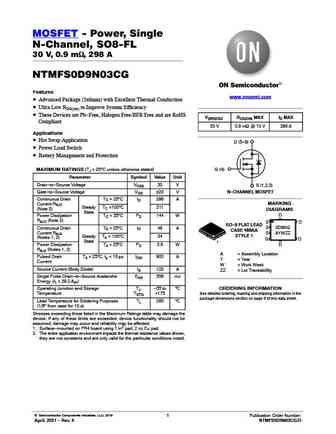
MOSFET - Power, Single N-Channel, SO8-FL 30 V, 0.9 mW, 298 A NTMFS0D9N03CG Features www.onsemi.com Advanced Package (5x6mm) with Excellent Thermal Conduction Ultra Low RDS(on) to Improve System Efficiency These Devices are Pb-Free, Halogen Free/BFR Free and are RoHS V(BR)DSS RDS(ON) MAX ID MAX Compliant 30 V 0.9 mW @ 10 V 298 A Applications Hot Swap Application D (
Otros transistores... NTMFD5C466NT1G
, NTMFD5C470NLT1G
, NTMFD5C650NLT1G
, NTMFD5C674NLT1G
, NTMFD6H840NLT1G
, NTMFD6H846NLT1G
, NTMFS006N12MCT1G
, NTMFS008N12MCT1G
, 5N60
, NTMFS0D8N02P1ET1G
, NTMFS0D9N03CGT1G
, NTMFS1D15N03CGT1G
, NTMFS1D7N03CGT1G
, NTMFS23D9N06HLT1G
, NTMFS3D6N10MCLT1G
, NTMFS4C05NT1G
, NTMFS4D2N10MDT1G
.