NCE20P07N MOSFET Equivalente. Reemplazo. Hoja de especificaciones. Principales características
Número de Parte: NCE20P07N
Tipo de FET: MOSFET
Polaridad de transistor: P
ESPECIFICACIONES MÁXIMAS
Pdⓘ - Máxima disipación de potencia: 1.5 W
|Vds|ⓘ - Voltaje máximo drenador-fuente: 20 V
|Vgs|ⓘ - Voltaje máximo fuente-puerta: 10 V
|Id|ⓘ - Corriente continua de drenaje: 7 A
Tjⓘ - Temperatura máxima de unión: 150 °C
CARACTERÍSTICAS ELÉCTRICAS
trⓘ - Tiempo de subida: 10 nS
Cossⓘ - Capacitancia de salida: 160 pF
RDSonⓘ - Resistencia estado encendido drenaje a fuente: 0.045 Ohm
Encapsulados: SOT23-6L
Búsqueda de reemplazo de NCE20P07N MOSFET
- Selecciónⓘ de transistores por parámetros
NCE20P07N datasheet
nce20p07n.pdf
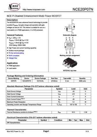
http //www.ncepower.com NCE20P07N NCE P-Channel Enhancement Mode Power MOSFET Description The NCE20P07N uses advanced trench technology to provide excellent RDS(ON), low gate charge and operation with gate voltages as low as1.8V. This device is suitable for use as a load switch or in PWM applications .It is ESD protested. Schematic diagram General Features VDS = -20V,ID =
nce20p05y.pdf
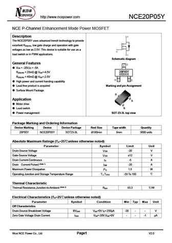
http //www.ncepower.com NCE20P05Y NCE P-Channel Enhancement Mode Power MOSFET Description The NCE20P05Y uses advanced trench technology to provide excellent R , low gate charge and operation with gate DS(ON) voltages as low as 2.5V. This device is suitable for use as a load switch or in PWM applications. Schematic diagram General Features V = -20V,I = -5A DS D R
nce20p08j.pdf

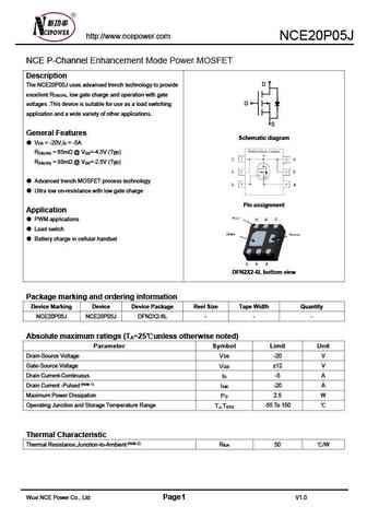
http //www.ncepower.com NCE20P08J NCE P-Channel Enhancement Mode Power MOSFET Description D The NCE20P08J uses advanced trench technology to provide excellent R , low gate charge and operation with gate DS(ON) G voltages .This device is suitable for use as a load switching application and a wide variety of other applications. S General Features Schematic diagram V = -20V,I = -
nce20p09s.pdf
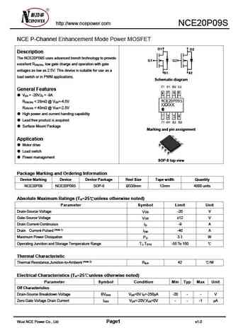
http //www.ncepower.com NCE20P09S NCE P-Channel Enhancement Mode Power MOSFET D1 D2 Description The NCE20P09S uses advanced trench technology to provide G1 G2 excellent R , low gate charge and operation with gate DS(ON) voltages as low as 2.5V. This device is suitable for use as a S1 S2 load switch or in PWM applications. Schematic diagram General Features V = -20V,I = -9A D
Otros transistores... NCE2014ES, NCE2025I, NCE2025S, NCE2030U, NCE2090K, NCE20NP1006S, NCE20P05J, NCE20P05Y, EMB04N03H, NCE20P08J, NCE20P09S, NCE20P10J, NCE20P85GU, NCE2301A, NCE2301B, NCE2301C, NCE2301D
🌐 : EN ES РУ

Liste
Recientemente añadidas las descripciónes de los transistores:
MOSFET: FTF30P35D | FTF25N35DHVT | FTF15N35D | FTE15C35G | FTP02P15G | FTE02P15G | AKF30N5P0SX | AKF30N10S | AKF20P45D | CM4407 | CM3407 | CM3400 | SVF11N65F | SVF11N65T | FKBB3105 | EHBA036R1
Popular searches
2sc2078 transistor | bc558 datasheet | p75nf75 mosfet | ao4407a | mpsa06 datasheet | bc548 pinout | bdw94c | bd140 transistor