NCE60P09AS MOSFET Equivalente. Reemplazo. Hoja de especificaciones. Principales características
Número de Parte: NCE60P09AS
Tipo de FET: MOSFET
Polaridad de transistor: P
ESPECIFICACIONES MÁXIMAS
Pdⓘ - Máxima
disipación de potencia: 3 W
|Vds|ⓘ - Voltaje máximo drenador-fuente: 60 V
|Vgs|ⓘ - Voltaje máximo fuente-puerta: 20 V
|Id|ⓘ - Corriente continua
de drenaje: 9 A
Tjⓘ - Temperatura máxima de unión: 150 °C
CARACTERÍSTICAS ELÉCTRICAS
trⓘ - Tiempo
de subida: 14 nS
Cossⓘ - Capacitancia de salida: 124.3 pF
RDSonⓘ - Resistencia estado encendido drenaje a fuente: 0.05 Ohm
Encapsulados: SOP8
Búsqueda de reemplazo de NCE60P09AS MOSFET
- Selecciónⓘ de transistores por parámetros
NCE60P09AS datasheet
..1. Size:288K ncepower
nce60p09as.pdf 
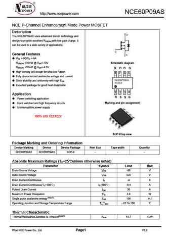
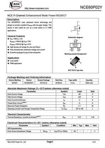
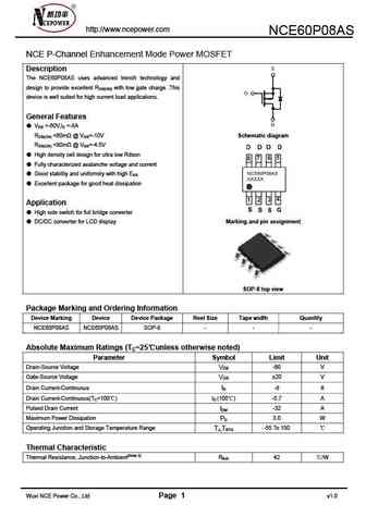
NCE60P09AS http //www.ncepower.com NCE P-Channel Enhancement Mode Power MOSFET Description The NCE60P09AS uses advanced trench technology and design to provide excellent RDS(ON) with low gate charge. It can be used in a wide variety of applications. General Features VDS =-60V,ID =-9A RDS(ON)
6.1. Size:285K ncepower
nce60p09s.pdf
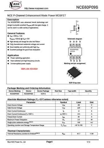
NCE60P09S http //www.ncepower.com NCE P-Channel Enhancement Mode Power MOSFET Description The NCE60P09S uses advanced trench technology and design to provide excellent RDS(ON) with low gate charge. It can be used in a wide variety of applications. General Features VDS =-60V,ID =-9A RDS(ON)
6.2. Size:655K ncepower
nce60p09k.pdf
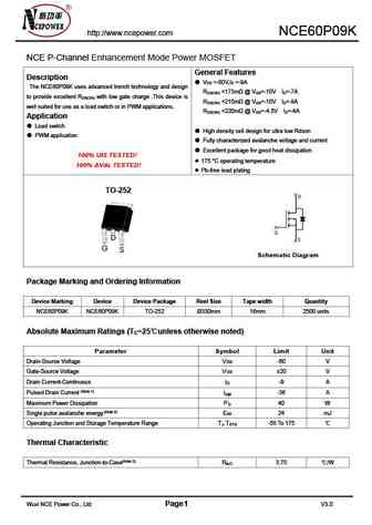
http //www.ncepower.com NCE60P09K NCE P-Channel Enhancement Mode Power MOSFET General Features Description V =-60V,I =-9A DS D The NCE60P09K uses advanced trench technology and design R
7.2. Size:411K ncepower
nce60p05n.pdf
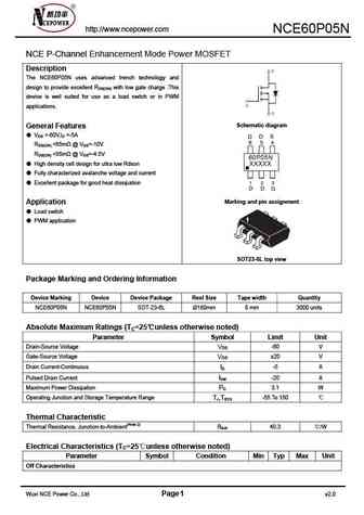
http //www.ncepower.com NCE60P05N NCE P-Channel Enhancement Mode Power MOSFET Description The NCE60P05N uses advanced trench technology and design to provide excellent RDS(ON) with low gate charge .This device is well suited for use as a load switch or in PWM applications. Schematic diagram General Features VDS =-60V,ID =-5A RDS(ON)
7.3. Size:364K ncepower
nce60p06s.pdf
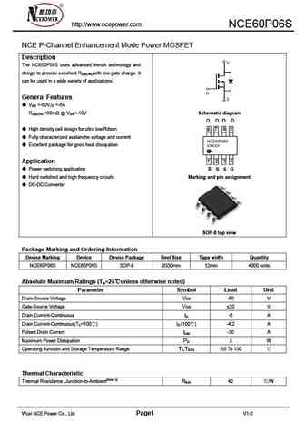
http //www.ncepower.com NCE60P06S NCE P-Channel Enhancement Mode Power MOSFET Description The NCE60P06S uses advanced trench technology and design to provide excellent RDS(ON) with low gate charge. It can be used in a wide variety of applications. General Features VDS =-60V,ID =-6A RDS(ON)
7.6. Size:656K ncepower
nce60p03r.pdf
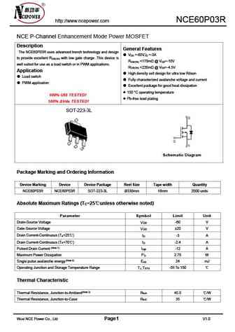
http //www.ncepower.com NCE60P03R NCE P-Channel Enhancement Mode Power MOSFET Description General Features The NCE60P03R uses advanced trench technology and design V =-60V,I =-3A DS D to provide excellent R with low gate charge .This device is DS(ON) R
7.7. Size:358K ncepower
nce60p04sn.pdf
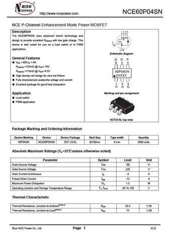
NCE60P04SN http //www.ncepower.com NCE P-Channel Enhancement Mode Power MOSFET Description The NCE60P04SN uses advanced trench technology and design to provide excellent RDS(ON) with low gate charge .This device is well suited for use as a load switch or in PWM applications. Schematic diagram General Features VDS =-60V,ID =-4A RDS(ON)
7.8. Size:492K ncepower
nce60p05r.pdf
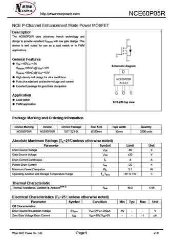
http //www.ncepower.com NCE60P05R NCE P-Channel Enhancement Mode Power MOSFET Description The NCE60P05R uses advanced trench technology and design to provide excellent RDS(ON) with low gate charge .This device is well suited for use as a load switch or in PWM applications. General Features VDS =-60V,ID =-5A Schematic diagram RDS(ON)
7.9. Size:371K ncepower
nce60p07as.pdf
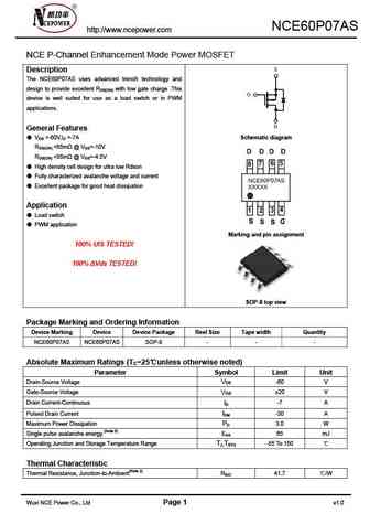
NCE60P07AS http //www.ncepower.com NCE P-Channel Enhancement Mode Power MOSFET Description The NCE60P07AS uses advanced trench technology and design to provide excellent RDS(ON) with low gate charge .This device is well suited for use as a load switch or in PWM applications. General Features VDS =-60V,ID =-7A Schematic diagram RDS(ON)
7.10. Size:344K ncepower
nce60p04y.pdf
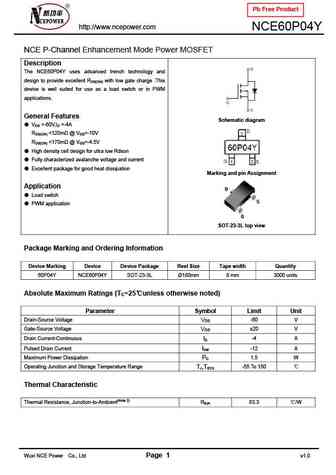
Pb Free Product http //www.ncepower.com NCE60P04Y NCE P-Channel Enhancement Mode Power MOSFET Description The NCE60P04Y uses advanced trench technology and design to provide excellent RDS(ON) with low gate charge .This device is well suited for use as a load switch or in PWM applications. General Features Schematic diagram VDS =-60V,ID =-4A RDS(ON)
7.11. Size:353K ncepower
nce60p03y.pdf
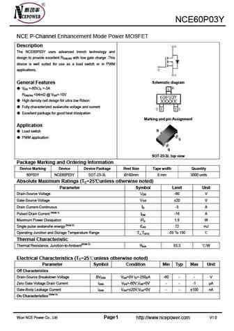
NCE60P03Y NCE P-Channel Enhancement Mode Power MOSFET Description The NCE60P03Y uses advanced trench technology and design to provide excellent RDS(ON) with low gate charge .This device is well suited for use as a load switch or in PWM applications. Schematic diagram General Features VDS =-60V,ID =-3A RDS(ON)
7.12. Size:333K ncepower
nce60p04r.pdf
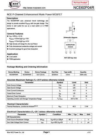
Pb Free Product http //www.ncepower.com NCE60P04R NCE P-Channel Enhancement Mode Power MOSFET Description The NCE60P04R uses advanced trench technology and design to provide excellent RDS(ON) with low gate charge .This device is well suited for use as a load switch or in PWM applications. General Features VDS =-60V,ID =-4.3A Schematic diagram RDS(ON)
Otros transistores... NCE60P03R, NCE60P03Y, NCE60P04SN, NCE60P05BY, NCE60P05N, NCE60P05R, NCE60P07AS, NCE60P08AS, IRF520, NCE60P09K, NCE60P12AS, NCE60P16AQ, NCE60P17AQ, NCE60P18AQ, NCE60P25, NCE60P28AK, NCE60P40F