NCE6890D MOSFET Equivalente. Reemplazo. Hoja de especificaciones. Principales características
Número de Parte: NCE6890D
Tipo de FET: MOSFET
Polaridad de transistor: N
ESPECIFICACIONES MÁXIMAS
Pdⓘ - Máxima disipación de potencia: 130 W
|Vds|ⓘ - Voltaje máximo drenador-fuente: 68 V
|Vgs|ⓘ - Voltaje máximo fuente-puerta: 20 V
|Id|ⓘ - Corriente continua de drenaje: 90 A
Tjⓘ - Temperatura máxima de unión: 175 °C
CARACTERÍSTICAS ELÉCTRICAS
trⓘ - Tiempo de subida: 94 nS
Cossⓘ - Capacitancia de salida: 450 pF
RDSonⓘ - Resistencia estado encendido drenaje a fuente: 0.0075 Ohm
Encapsulados: TO-263
Búsqueda de reemplazo de NCE6890D MOSFET
- Selecciónⓘ de transistores por parámetros
NCE6890D datasheet
nce6890d.pdf
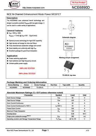
Pb Free Product http //www.ncepower.com NCE6890D NCE N-Channel Enhancement Mode Power MOSFET Description The NCE6890D uses advanced trench technology and design to provide excellent RDS(ON) with low gate charge. It can be used in a wide variety of applications. General Features VDS = 68V,ID =90A RDS(ON)
nce6890k.pdf
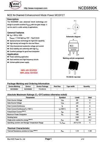
http //www.ncepower.com NCE6890K NCE N-Channel Enhancement Mode Power MOSFET Description The NCE6890K uses advanced trench technology and design to provide excellent RDS(ON) with low gate charge. It can be used in a wide variety of applications. General Features VDS = 68V,ID =90A Schematic diagram RDS(ON)
nce6890.pdf
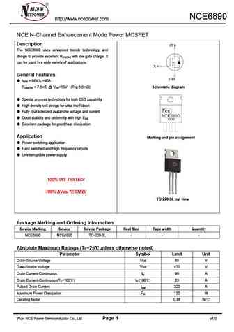
NCE6890 http //www.ncepower.com NCE N-Channel Enhancement Mode Power MOSFET Description The NCE6890 uses advanced trench technology and design to provide excellent RDS(ON) with low gate charge. It can be used in a wide variety of applications. General Features VDS = 68V,ID =90A RDS(ON)
nce6802.pdf
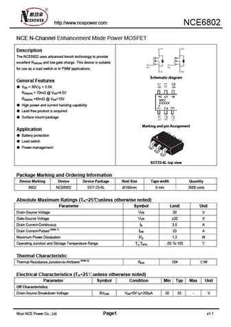
http //www.ncepower.com NCE6802 NCE N-Channel Enhancement Mode Power MOSFET Description The NCE6802 uses advanced trench technology to provide excellent RDS(ON) and low gate charge .This device is suitable for use as a load switch or in PWM applications. Schematic diagram General Features VDS = 30V,ID = 3.5A RDS(ON)
Otros transistores... NCE65NF190T, NCE65NF190V, NCE65T130T, NCE65T180V, NCE65T1K9I, NCE65T1K9K, NCE65TF078T, NCE6602N, IRFB31N20D, NCE70H10F, NCE70N100I, NCE70N1K1D, NCE70N1K1F, NCE70N1K1I, NCE70N1K1K, NCE70N1K1R, NCE70N1K4F
🌐 : EN ES РУ

Liste
Recientemente añadidas las descripciónes de los transistores:
MOSFET: FTF30P35D | FTF25N35DHVT | FTF15N35D | FTE15C35G | FTP02P15G | FTE02P15G | AKF30N5P0SX | AKF30N10S | AKF20P45D | CM4407 | CM3407 | CM3400 | SVF11N65F | SVF11N65T | FKBB3105 | EHBA036R1
Popular searches
2sc2383 | c3198 transistor | irfb3607pbf datasheet | 60n60 | 2n5485 equivalent | 2sa1941 | 2sc485 | 2sd287