NCEP020N85D Datasheet. Equivalente. Reemplazo. Hoja de especificaciones. Principales características
Número de Parte: NCEP020N85D
Tipo de FET: MOSFET
Polaridad de transistor: N
ESPECIFICACIONES MÁXIMAS
Pdⓘ - Máxima disipación de potencia: 340 W
|Vds|ⓘ - Voltaje máximo drenador-fuente: 85 V
|Vgs|ⓘ - Voltaje máximo fuente-puerta: 20 V
|Id|ⓘ - Corriente continua de drenaje: 300 A
Tjⓘ - Temperatura máxima de unión: 175 °C
CARACTERÍSTICAS ELÉCTRICAS
trⓘ - Tiempo de subida: 39 nS
Cossⓘ - Capacitancia de salida: 2450 pF
RDSonⓘ - Resistencia estado encendido drenaje a fuente: 0.002 Ohm
Encapsulados: TO-263
Búsqueda de reemplazo de NCEP020N85D MOSFET
- Selecciónⓘ de transistores por parámetros
NCEP020N85D datasheet
ncep020n85d.pdf

NCEP020N85, NCEP020N85D NCE N-Channel Super Trench II Power MOSFET Description The series of devices uses Super Trench II technology that is General Features uniquely optimized to provide the most efficient high frequency VDS =85V,ID =300A switching performance. Both conduction and switching power RDS(ON)=1.8m , typical (TO-220)@ VGS=10V losses are minimized due to an ext
ncep020n85 ncep020n85d.pdf
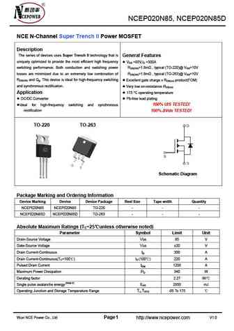
NCEP020N85, NCEP020N85D NCE N-Channel Super Trench II Power MOSFET Description The series of devices uses Super Trench II technology that is General Features uniquely optimized to provide the most efficient high frequency VDS =85V,ID =300A switching performance. Both conduction and switching power RDS(ON)=1.8m , typical (TO-220)@ VGS=10V losses are minimized due to an ext
ncep020n85ll.pdf
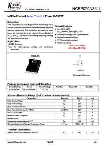
http //www.ncepower.com NCEP020N85LL NCE N-Channel Super Trench II Power MOSFET Description The series of devices uses Super Trench II technology that is General Features uniquely optimized to provide the most efficient high frequency V =85V,I =295A DS D switching performance. Both conduction and switching power R =1.6m , typical @ V =10V DS(ON) GS losses are minimized due to a
ncep020n85.pdf

NCEP020N85, NCEP020N85D NCE N-Channel Super Trench II Power MOSFET Description The series of devices uses Super Trench II technology that is General Features uniquely optimized to provide the most efficient high frequency VDS =85V,ID =300A switching performance. Both conduction and switching power RDS(ON)=1.8m , typical (TO-220)@ VGS=10V losses are minimized due to an ext
Otros transistores... NCEP01T25T, NCEP01T30T, NCEP020N10LL, NCEP020N30BQU, NCEP020N30QU, NCEP020N60AGU, NCEP020N60GU, NCEP020N85, IRFZ46N, NCEP020N85LL, NCEP020N85T, NCEP0210Q, NCEP0212F, NCEP0218G, NCEP0218K, NCEP0220F, NCEP0225F
🌐 : EN ES РУ

Liste
Recientemente añadidas las descripciónes de los transistores:
MOSFET: FTF30P35D | FTF25N35DHVT | FTF15N35D | FTE15C35G | FTP02P15G | FTE02P15G | AKF30N5P0SX | AKF30N10S | AKF20P45D | CM4407 | CM3407 | CM3400 | SVF11N65F | SVF11N65T | FKBB3105 | EHBA036R1
Popular searches
ksa1015yta | 2n4240 | 2n5210 transistor | toshiba 2sc2290 | pk6d0ba mosfet | 2sd726 | c536 transistor equivalent | 2sa1294 datasheet