NCEP050N10MG Datasheet. Equivalente. Reemplazo. Hoja de especificaciones. Principales características
Número de Parte: NCEP050N10MG
Tipo de FET: MOSFET
Polaridad de transistor: N
ESPECIFICACIONES MÁXIMAS
Pdⓘ - Máxima disipación de potencia: 145 W
|Vds|ⓘ - Voltaje máximo drenador-fuente: 100 V
|Vgs|ⓘ - Voltaje máximo fuente-puerta: 20 V
|Id|ⓘ - Corriente continua de drenaje: 120 A
Tjⓘ - Temperatura máxima de unión: 150 °C
CARACTERÍSTICAS ELÉCTRICAS
trⓘ - Tiempo de subida: 61 nS
Cossⓘ - Capacitancia de salida: 540 pF
RDSonⓘ - Resistencia estado encendido drenaje a fuente: 0.005 Ohm
Encapsulados: PDFN5X6-8L
Búsqueda de reemplazo de NCEP050N10MG MOSFET
- Selecciónⓘ de transistores por parámetros
NCEP050N10MG datasheet
ncep050n10mg.pdf
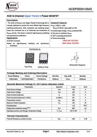
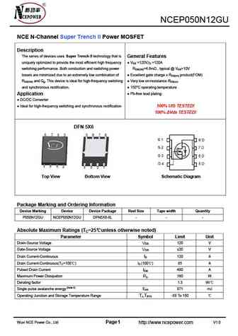
NCEP050N10MG NCE N-Channel Super Trench II Power MOSFET Description The series of devices uses Super Trench II technology that is General Features uniquely optimized to provide the most efficient high frequency V =100V,I =120A DS D switching performance. Both conduction and switching power R =4.45m , typical @ V =10V DS(ON) GS losses are minimized due to an extremely low combina
ncep050n10m.pdf
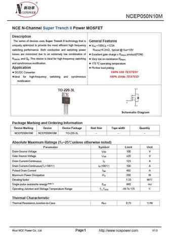
NCEP050N10M NCE N-Channel Super Trench II Power MOSFET Description The series of devices uses Super Trench II technology that is General Features uniquely optimized to provide the most efficient high frequency V =100V,I =123A DS D switching performance. Both conduction and switching power R =4.2m , typical @ V =10V DS(ON) GS losses are minimized due to an extremely low combinati
ncep050n10md.pdf
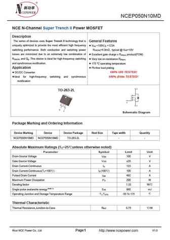
NCEP050N10MD NCE N-Channel Super Trench II Power MOSFET Description The series of devices uses Super Trench II technology that is General Features uniquely optimized to provide the most efficient high frequency V =100V,I =123A DS D switching performance. Both conduction and switching power R =4.0m , typical @ V =10V DS(ON) GS losses are minimized due to an extremely low combinat
ncep050n12d.pdf
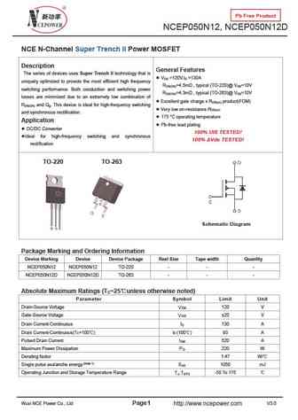
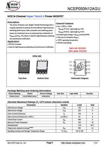
Pb Free Product NCEP050N12, NCEP050N12D NCE N-Channel Super Trench II Power MOSFET Description General Features The series of devices uses Super Trench II technology that is V =120V,I =130A DS D uniquely optimized to provide the most efficient high frequency R =4.5m , typical (TO-220)@ V =10V DS(ON) GS switching performance. Both conduction and switching power R =4.3m , typi


Otros transistores... NCEP048N85D, NCEP048N85M, NCEP048N85MD, NCEP048NH150, NCEP048NH150D, NCEP048NH150T, NCEP050N10M, NCEP050N10MD, IRFB7545, NCEP050N12, NCEP050N12AGU, NCEP050N12D, NCEP050N12GU, NCEP050N85G, NCEP050N85M, NCEP053N85GU, NCEP055N10
🌐 : EN ES РУ

Liste
Recientemente añadidas las descripciónes de los transistores:
MOSFET: RM50P30DF | CRTT095N12N | CRSS028N10N | CRST030N10N | CRJQ80N65F | ASDM20N20KQ | ASDM20N100Q | ASDM12N65F | ASDM100R750PKQ | ASDM100R160NKQ | ASDM100R090NP | ASDM100R066NQ | ASDM100R045NQ | ASDM100N34KQ | ASDM100N15KQ | FTF30P35D
Popular searches
k389 transistor | mje15032g equivalent | nsd134 | 60r190p datasheet | cs30n20 datasheet | go42n10 | 2sa970 datasheet | 2sc1627