NCEP070N12 Datasheet. Equivalente. Reemplazo. Hoja de especificaciones. Principales características
Número de Parte: NCEP070N12
Tipo de FET: MOSFET
Polaridad de transistor: N
ESPECIFICACIONES MÁXIMAS
Pdⓘ - Máxima disipación de potencia: 150 W
|Vds|ⓘ - Voltaje máximo drenador-fuente: 120 V
|Vgs|ⓘ - Voltaje máximo fuente-puerta: 20 V
|Id|ⓘ - Corriente continua de drenaje: 100 A
Tjⓘ - Temperatura máxima de unión: 175 °C
CARACTERÍSTICAS ELÉCTRICAS
trⓘ - Tiempo de subida: 15 nS
Cossⓘ - Capacitancia de salida: 390 pF
RDSonⓘ - Resistencia estado encendido drenaje a fuente: 0.007 Ohm
Encapsulados: TO-220
Búsqueda de reemplazo de NCEP070N12 MOSFET
- Selecciónⓘ de transistores por parámetros
NCEP070N12 datasheet
ncep070n12.pdf

NCEP070N12,NCEP070N12D NCE N-Channel Super Trench II Power MOSFET Description General Features The series of devices uses Super Trench II technology that is VDS =120V,ID =100A uniquely optimized to provide the most efficient high frequency RDS(ON)=6.5m , typical (TO-220)@ VGS=10V switching performance. Both conduction and switching power RDS(ON)=6.3m , typical (TO-26
ncep070n12 ncep070n12d.pdf

NCEP070N12,NCEP070N12D NCE N-Channel Super Trench II Power MOSFET Description General Features The series of devices uses Super Trench II technology that is VDS =120V,ID =100A uniquely optimized to provide the most efficient high frequency RDS(ON)=6.5m , typical (TO-220)@ VGS=10V switching performance. Both conduction and switching power RDS(ON)=6.3m , typical (TO-26
ncep070n12d.pdf
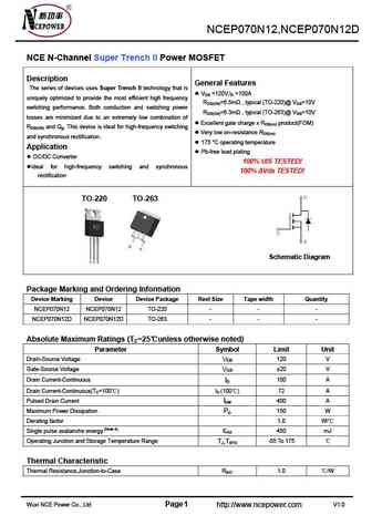
NCEP070N12,NCEP070N12D NCE N-Channel Super Trench II Power MOSFET Description General Features The series of devices uses Super Trench II technology that is VDS =120V,ID =100A uniquely optimized to provide the most efficient high frequency RDS(ON)=6.5m , typical (TO-220)@ VGS=10V switching performance. Both conduction and switching power RDS(ON)=6.3m , typical (TO-26
ncep070n10agu.pdf
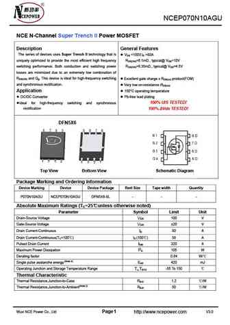
NCEP070N10AGU NCE N-Channel Super Trench II Power MOSFET Description General Features The series of devices uses Super Trench II technology that is VDS =100V,ID =80A uniquely optimized to provide the most efficient high frequency RDS(ON)=6.1m , typical@ VGS=10V switching performance. Both conduction and switching power RDS(ON)=8.35m , typical@ VGS=4.5V losses are minimiz
Otros transistores... NCEP065N10AGU, NCEP065N10AK, NCEP065N10GU, NCEP065N12AGU, NCEP065N85D, NCEP068N10K, NCEP070N10AGU, NCEP070N10GU, IRF630, NCEP070N12D, NCEP072N10A, NCEP075N85AGU, NCEP075N85GU, NCEP078N10AG, NCEP078N10AK, NCEP078N10G, NCEP080N10
🌐 : EN ES РУ

Liste
Recientemente añadidas las descripciónes de los transistores:
MOSFET: ASDM40N60KQ | ASDM40N40E | ASDM40N100P | ASDM40DN20E | ASDM3416EZA | ASDM3415ZA | ASDM3401ZA | ASDM3401 | ASDM3400ZA | ASDM30P30BE | RM50P30DF | CRTT095N12N | CRSS028N10N | CRST030N10N | CRJQ80N65F | ASDM20N20KQ
Popular searches
2n5551 | irf540n | irf3205 mosfet | 2n3055 | irfp260n | 2n2222 datasheet | irf9540 | 2n3055 datasheet