FIR10N10LG MOSFET Equivalente. Reemplazo. Hoja de especificaciones. Principales características
Número de Parte: FIR10N10LG
Tipo de FET: MOSFET
Polaridad de transistor: N
ESPECIFICACIONES MÁXIMAS
Pdⓘ - Máxima disipación de potencia: 30 W
|Vds|ⓘ - Voltaje máximo drenador-fuente: 100 V
|Vgs|ⓘ - Voltaje máximo fuente-puerta: 20 V
|Id|ⓘ - Corriente continua de drenaje: 10 A
Tjⓘ - Temperatura máxima de unión: 150 °C
CARACTERÍSTICAS ELÉCTRICAS
trⓘ - Tiempo de subida: 7.4 nS
Cossⓘ - Capacitancia de salida: 120 pF
RDSonⓘ - Resistencia estado encendido drenaje a fuente: 0.21 Ohm
Encapsulados: TO-252
Búsqueda de reemplazo de FIR10N10LG MOSFET
- Selecciónⓘ de transistores por parámetros
FIR10N10LG datasheet
fir10n10lg.pdf
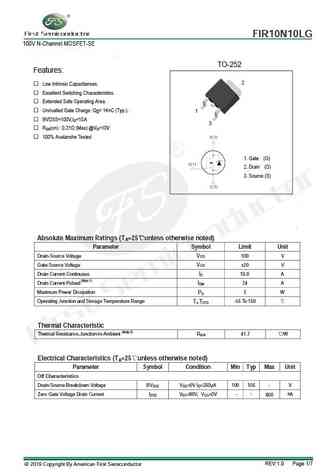
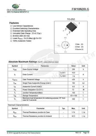
FIR10N10LG 100V N-Channel MOSFET-SE TO-252 Features 2 Low Intrinsic Capacitances. Excellent Switching Characteristics. Extended Safe Operating Area. Unrivalled Gate Charge Qg= 14nC (Typ.). 1 BVDSS=100V,ID=10A 3 RDS(on) 0.21 (Max) @VG=10V 100% Avalanche Tested 1. Gate (G) 2. Drain (D) 3. Source (S) Absolute Maximum Ratings (TA=25 un
fir10n50fg.pdf
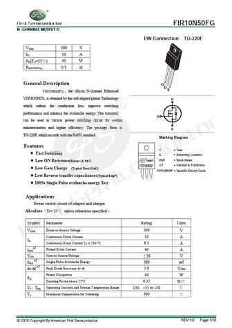
FIR10N50FG N - CHANNEL MOSFET-G PIN Connection TO-220F VDSS 500 V ID 10 A PD(TC=25 ) 40 W RDS(ON)Typ 0.5 General Description G D S , the silicon N-channel Enhanced FIR10N50FG VDMOSFETs, is obtained by the self-aligned planar Technology D which reduce the conduction loss, improve switching performance and enhance the avalanche energy. The transistor G can be
fir10n70fg.pdf
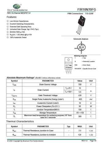
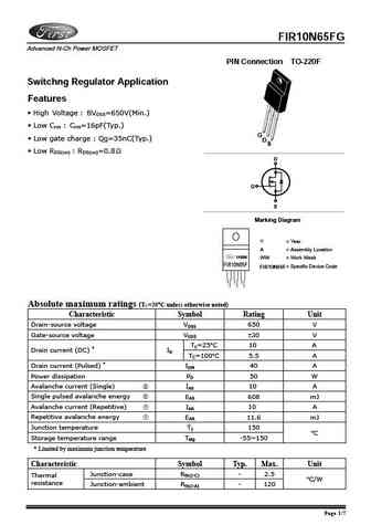
FIR10N70FG 700V N-Channel MOSFET-G PIN Connection TO-220F Features Low Intrinsic Capacitances. Excellent Switching Characteristics. Extended Safe Operating Area. Unrivalled Gate Charge Qg= 37nC (Typ.). BVDSS=700V,ID=10A G DS RDS(on) 1.0 (Max) @VG=10V 100% Avalanche Tested g Schematic dia ram D G S Marking Diagram Y = Year A = Assembly Locati
fir10n80fg.pdf
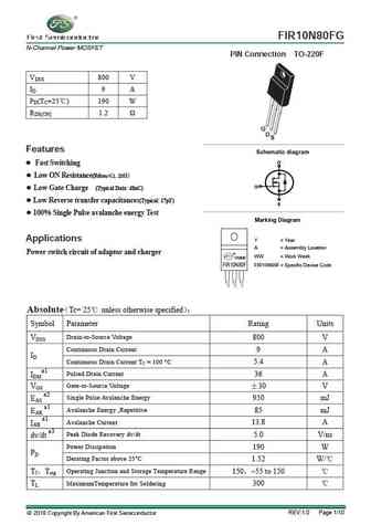
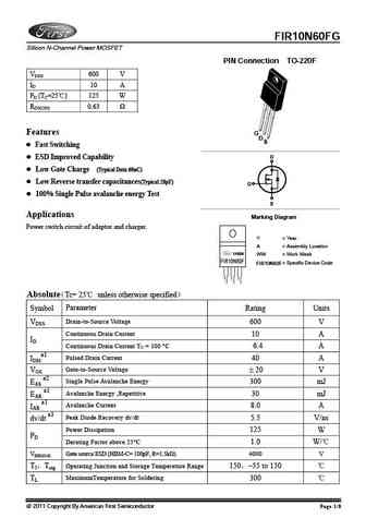
FIR10N80FG N-Channel Power MOSFET PIN Connection TO-220F VDSS 800 V ID 9 A PD(TC=25 ) 190 W RDS(ON) 1.2 G D S Features g Schematic dia ram D Fast Switching Low ON Resistance(Rdson 1.20 ) G Low Gate Charge (Typical Data 48nC) Low Reverse transfer capacitances(Typical 17pF) S 100% Single Pulse avalanche energy Test Marking Diagram Applications Y
Otros transistores... FDM20R120AN4G, FDM30R650AN4G, FDM40R120AN4G, FDM50R120AN4G, FDM60R65AN4G, FDM80R120AN4G, FDZ65T300D8G, FDZ90T150PG, IRF740, FIR10N20LG, FIR10N50FG, FIR10N70FG, FIR10N80FG, FIR110N10PG, FIR11N40FG, FIR11N90ANG, FIR11NS65AFG
🌐 : EN ES РУ

Liste
Recientemente añadidas las descripciónes de los transistores:
MOSFET: CM4407 | CM3407 | CM3400 | SVF11N65F | SVF11N65T | FKBB3105 | EHBA036R1 | CRTT067N10N | AP6NA3R2MT | AP65SA145DDT8 | AP4NAR95CMT-A | AP4024GEMT-HF | AP3P050AH | AP3P020H | AP3N9R5YT | AP3N9R5MT
Popular searches
a1491 transistor | 2sc897 | 2sa818 | 2sa763 | a933 | 2sa818 replacement | irfb3607 datasheet | 2n2907 equivalent