FIR120N08PG MOSFET Equivalente. Reemplazo. Hoja de especificaciones. Principales características
Número de Parte: FIR120N08PG
Tipo de FET: MOSFET
Polaridad de transistor: N
ESPECIFICACIONES MÁXIMAS
Pdⓘ - Máxima disipación de potencia: 220 W
|Vds|ⓘ - Voltaje máximo drenador-fuente: 80 V
|Vgs|ⓘ - Voltaje máximo fuente-puerta: 20 V
|Id|ⓘ - Corriente continua de drenaje: 120 A
Tjⓘ - Temperatura máxima de unión: 150 °C
CARACTERÍSTICAS ELÉCTRICAS
trⓘ - Tiempo de subida: 38 nS
Cossⓘ - Capacitancia de salida: 546 pF
RDSonⓘ - Resistencia estado encendido drenaje a fuente: 0.0055 Ohm
Encapsulados: TO-220AB
Búsqueda de reemplazo de FIR120N08PG MOSFET
- Selecciónⓘ de transistores por parámetros
FIR120N08PG datasheet
fir120n08pg.pdf
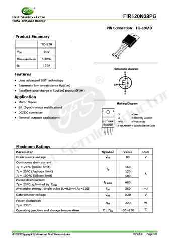
FIR120N08PG 120AN - CHANNEL MOSFET PIN Connection TO-220AB Product Summary TO-220 VDS 80V RDS(on)@VGS=10V 4.9m I 120A D Schematic diagram D Features Uses advanced SGT technology G Extremely low on-resistance RDS(on) Excellent gate charge x RDS(on) product(FOM) S Application Motor Drives Marking Diagram SR (Synchronous rectification) DC/DC conv
fir120n055pg.pdf
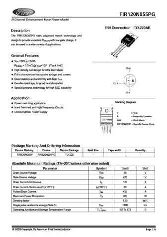
FIR120N055PG N-Channel Enhancement Mode Power Mosfet PIN Connection TO-220AB Description The FIR120N055PG uses advanced trench technology and design to provide excellent RDS(ON) with low gate charge. It can be used in a wide variety of applications. General Features VDS =55V,ID =120A RDS(ON)
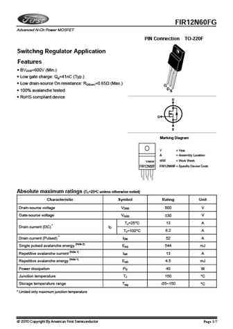
fir12n65fg.pdf
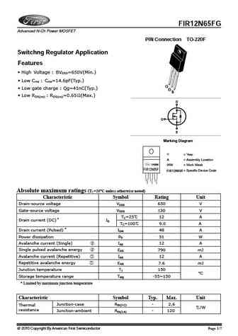
FIR12N65FG Advanced N-Ch Power MOSFET PIN Connection TO-220F Switchng Regulator Application Features High Voltage BVDSS=650V(Min.) Low Crss Crss=14.6pF(Typ.) G Low gate charge Qg=41nC(Typ.) D S Low RDS(on) RDS(on)=0.65 (Max.) D G S Marking Diagram Y = Year A = Assembly Location YAWW WW = Work Week FIR12N65F FIR12N65F = Specific Device C
fir12n15lg.pdf
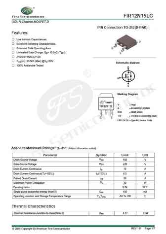
FIR12N15LG 150V N-Channel MOSFET-D PIN Connection TO-252(D-PAK) Features Low Intrinsic Capacitances. D Excellent Switching Characteristics. Extended Safe Operating Area. G Unrivalled Gate Charge Qg= 15.5nC (Typ.). S BVDSS=150V,ID=12A RDS(on) 0.29 (Max) @VG=10V g Schematic dia ram 100% Avalanche Tested D G S Marking Diagram YAWWVT Y =
Otros transistores... FIR10N50FG, FIR10N70FG, FIR10N80FG, FIR110N10PG, FIR11N40FG, FIR11N90ANG, FIR11NS65AFG, FIR11NS70AFG, IRLZ44N, FIR12N15LG, FIR12N70FG, FIR12N80FG, FIR13N50FG, FIR14N50FG, FIR14N65FG, FIR14NS65AFG, FIR14NS70AFG
History: IPI90N04S4-02
🌐 : EN ES РУ

Liste
Recientemente añadidas las descripciónes de los transistores:
MOSFET: CM4407 | CM3407 | CM3400 | SVF11N65F | SVF11N65T | FKBB3105 | EHBA036R1 | CRTT067N10N | AP6NA3R2MT | AP65SA145DDT8 | AP4NAR95CMT-A | AP4024GEMT-HF | AP3P050AH | AP3P020H | AP3N9R5YT | AP3N9R5MT
Popular searches
13009 transistor | irf3205 equivalent | ksa992 transistor | 2n2926 | ksa992 pinout | 2n1308 transistor | p609 | bc327-40