PA567JA Datasheet. Equivalente. Reemplazo. Hoja de especificaciones. Principales características
Número de Parte: PA567JA 📄📄
Tipo de FET: MOSFET
Polaridad de transistor: P
ESPECIFICACIONES MÁXIMAS
Pdⓘ - Máxima disipación de potencia: 0.41 W
|Vds|ⓘ - Voltaje máximo drenador-fuente: 20 V
|Vgs|ⓘ - Voltaje máximo fuente-puerta: 12 V
|Id|ⓘ - Corriente continua de drenaje: 0.68 A
Tjⓘ - Temperatura máxima de unión: 150 °C
CARACTERÍSTICAS ELÉCTRICAS
trⓘ - Tiempo de subida: 30 nS
Cossⓘ - Capacitancia de salida: 18 pF
RDSonⓘ - Resistencia estado encendido drenaje a fuente: 0.52 Ohm
Encapsulados: SOT-23-6
📄📄 Copiar
Búsqueda de reemplazo de PA567JA MOSFET
- Selecciónⓘ de transistores por parámetros
PA567JA datasheet
pa567ja.pdf
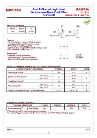
Dual P-Channel Logic Level PA567JA NIKO-SEM Enhancement Mode Field Effect SOT-23-6 Transistor Halogen-Free & Lead-Free PRODUCT SUMMARY V(BR)DSS RDS(ON) ID -20V 520m -0.68A Features Pb-Free, Halogen Free and RoHS compliant. Low RDS(on) to Minimize Conduction Losses. Ohmic Region Good RDS(on) Ratio. Optimized Gate Charge to Minimize Switching Losses.
pa567ea.pdf
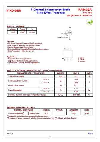
P-Channel Enhancement Mode PA567EA NIKO-SEM SOT-23-6 Field Effect Transistor Halogen-Free & Lead-Free PRODUCT SUMMARY V(BR)DSS RDS(ON) ID -20V 520m -0.68A Features Pb-Free, Halogen Free and RoHS compliant. Low RDS(on) to Minimize Conduction Losses. Ohmic Region Good RDS(on) Ratio. Optimized Gate Charge to Minimize Switching Losses. ESD Protecti
Otros transistores... PA110ED, PA110HEA, PA110NK, PA110NV, PA410BTF, PA515BD, PA520BA, PA567EA, IRF4905, PA597BA, PA5D8EA, PA5D8JA, PA5S6EA, PA5S6JA, PA607UA, PA710ED, PA910BC
Parámetros del MOSFET. Cómo se afectan entre sí.
History: STD9NM50N | AGM15T13H | AO4828 | JMSH040SAGQ | FDB8442F085 | SSFM8005 | HGP045N15S
🌐 : EN ES РУ

Liste
Recientemente añadidas las descripciónes de los transistores:
MOSFET: CS95118 | CS85105A | CS75N45 | CS72N12 | CS55N50 | CS48N75A | CS40N27 | MSQ60P04D | MSQ40P07D | MSQ30P40D | MSQ30P15 | MSQ30P07D | MSQ100N03D | MSHM60P14 | MSHM40N085 | MSHM30N46
Popular searches
2sd665 | 7506 mosfet datasheet | 2sb1186a | a1695 datasheet | 3415 transistor | 072ne6pt | 2sd388 | 2sc1400