D2N60 MOSFET Equivalente. Reemplazo. Hoja de especificaciones. Principales características
Número de Parte: D2N60
Tipo de FET: MOSFET
Polaridad de transistor: N
ESPECIFICACIONES MÁXIMAS
Pdⓘ - Máxima
disipación de potencia: 35 W
|Vds|ⓘ - Voltaje máximo drenador-fuente: 600 V
|Vgs|ⓘ - Voltaje máximo fuente-puerta: 30 V
|Id|ⓘ - Corriente continua
de drenaje: 2 A
Tjⓘ - Temperatura máxima de unión: 150 °C
CARACTERÍSTICAS ELÉCTRICAS
trⓘ - Tiempo
de subida: 13 nS
Cossⓘ - Capacitancia de salida: 33 pF
RDSonⓘ - Resistencia estado encendido drenaje a fuente: 4.5 Ohm
Encapsulados: TO252
Búsqueda de reemplazo de D2N60 MOSFET
- Selecciónⓘ de transistores por parámetros
D2N60 datasheet
..1. Size:1285K cn wxdh
d2n60.pdf 
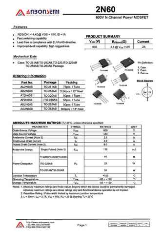
D2N60 2A 600V N-channel Enhancement Mode Power MOSFET 1 Description These N-channel enhanced vdmosfets, is obtained by the self-aligned V DSS = 600V planar technology which reduce the conduction loss, improve switching I = 2.0A D performance and enhance the avalanche energy. Which accords with the RoHS standard. R DS(on) TYP) =3.6 Fast switching ESD improved capabilit
0.1. Size:75K philips
php2n60e phb2n60e phd2n60e.pdf
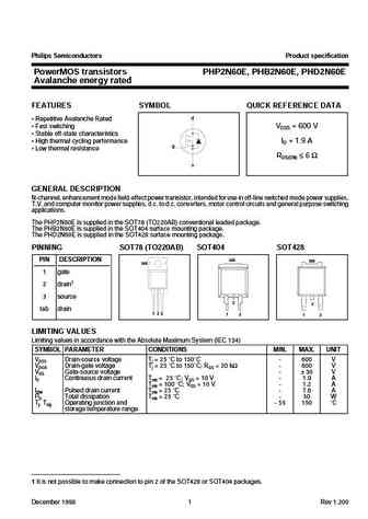
Philips Semiconductors Product specification PowerMOS transistors PHP2N60E, PHB2N60E, PHD2N60E Avalanche energy rated FEATURES SYMBOL QUICK REFERENCE DATA d Repetitive Avalanche Rated Fast switching VDSS = 600 V Stable off-state characteristics High thermal cycling performance ID = 1.9 A g Low thermal resistance RDS(ON) 6 s GENERAL DESCRIPTION N-chan
0.2. Size:762K fairchild semi
fqd2n60c fqu2n60c fqu2n60ctu.pdf
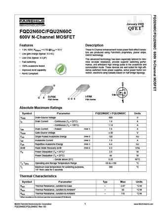
January 2009 QFET FQD2N60C/FQU2N60C 600V N-Channel MOSFET Features Description 1.9A, 600V, RDS(on) = 4.7 @VGS = 10 V These N-Channel enhancement mode power field effect transis- tors are produced using Fairchild s proprietary, planar stripe, Low gate charge (typical 8.5 nC) DMOS technology. Low Crss (typical 4.3 pF) This advanced technology has been especially tail
0.3. Size:560K fairchild semi
fqd2n60tf fqd2n60tm fqu2n60tu.pdf
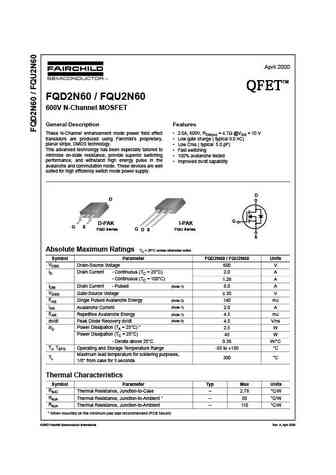
April 2000 TM QFET QFET QFET QFET FQD2N60 / FQU2N60 600V N-Channel MOSFET General Description Features These N-Channel enhancement mode power field effect 2.0A, 600V, RDS(on) = 4.7 @VGS = 10 V transistors are produced using Fairchild s proprietary, Low gate charge ( typical 9.0 nC) planar stripe, DMOS technology. Low Crss ( typical 5.0 pF) This advanced technology
0.4. Size:557K fairchild semi
fqd2n60ctm.pdf
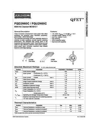
November 2013 FQD2N60C / FQU2N60C N-Channel QFET MOSFET 600 V, 1.9 A, 4.7 Features Description 1.9 A, 600 V, RDS(on) = 4.7 (Max.) @ VGS = 10 V, This N-Channel enhancement mode power MOSFET is ID = 0.95 A produced using Fairchild Semiconductor s proprietary Low Gate Charge (Typ. 8.5 nC) planar stripe and DMOS technology. This advanced Low Crss (Typ. 4.3 pF)
0.5. Size:618K onsemi
fqd2n60c fqu2n60c.pdf
TM QFET FQD2N60C / FQU2N60C 600V N-Channel MOSFET General Description Features These N-Channel enhancement mode power field effect 1.9A, 600V, RDS(on) = 4.7 @VGS = 10 V transistors are produced using Fairchild s proprietary, Low gate charge ( typical 8.5 nC) planar stripe, DMOS technology. Low Crss ( typical 4.3 pF) This advanced technology has been especially tailored
0.6. Size:49K kec
kmb8d2n60qa.pdf
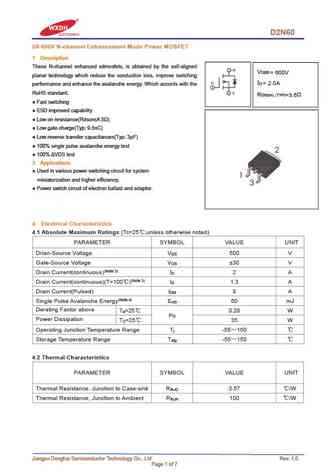
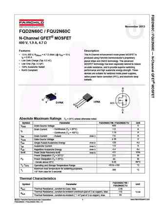
SEMICONDUCTOR KMB8D2N60QA TECHNICAL DATA N-Ch Trench MOSFET GENERAL DESCRIPTION This Trench MOSFET has better characteristics, such as fast switching time, low on resistance, low gate charge and excellent avalanche characteristiscs. It is mainly suitable for Back-light Inverter. H T D P G L FEATURES VDSS=60V, ID=8.2A. A Drain-Source ON Resistance. DIM MILLIMETERS A _ + RDS(ON)=
0.7. Size:428K aosemi
aod2n60a aoi2n60a aou2n60a.pdf
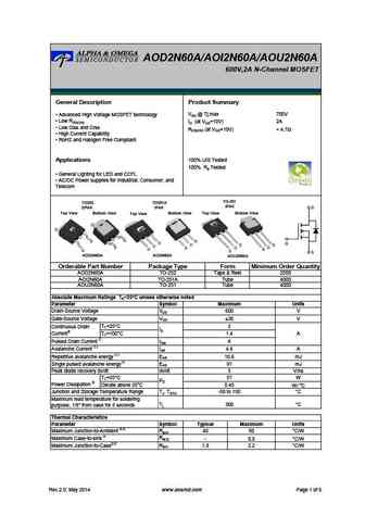
AOD2N60A/AOI2N60A/AOU2N60A 600V,2A N-Channel MOSFET General Description Product Summary VDS @ Tj,max 700V Advanced High Voltage MOSFET technology Low RDS(ON) ID (at VGS=10V) 2A Low Ciss and Crss RDS(ON) (at VGS=10V)
0.8. Size:327K aosemi
aod2n60.pdf
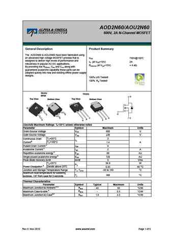
AOD2N60/AOU2N60 600V, 2A N-Channel MOSFET General Description Product Summary The AOD2N60 & AOU2N60 have been fabricated using an advanced high voltage MOSFET process that is VDS 700V@150 designed to deliver high levels of performance and ID (at VGS=10V) 2A robustness in popular AC-DC applications. RDS(ON) (at VGS=10V)
0.9. Size:368K aosemi
aod2n60 aou2n60.pdf
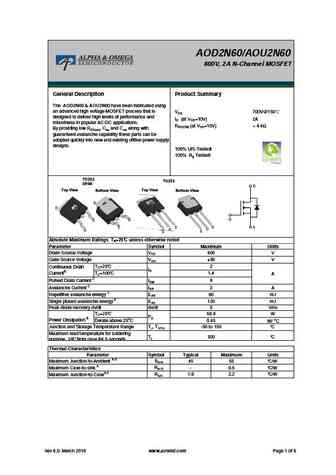
AOD2N60/AOU2N60 600V, 2A N-Channel MOSFET General Description Product Summary The AOD2N60 & AOU2N60 have been fabricated using an advanced high voltage MOSFET process that is VDS 700V@150 designed to deliver high levels of performance and ID (at VGS=10V) 2A robustness in popular AC-DC applications. RDS(ON) (at VGS=10V)
0.10. Size:428K aosemi
aod2n60a.pdf

AOD2N60A/AOI2N60A/AOU2N60A 600V,2A N-Channel MOSFET General Description Product Summary VDS @ Tj,max 700V Advanced High Voltage MOSFET technology Low RDS(ON) ID (at VGS=10V) 2A Low Ciss and Crss RDS(ON) (at VGS=10V)
0.11. Size:681K blue-rocket-elect
brd2n60.pdf
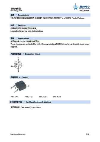
BRD2N60 Rev.D May.-2016 DATA SHEET / Descriptions TO-252 N MOS N-CHANNEL MOSFET in a TO-252 Plastic Package. / Features , , Low gate charge, low crss, fast switching. / Applications DC/DC These devices are well suited for high efficiency
0.12. Size:603K silan
svd2n60.pdf
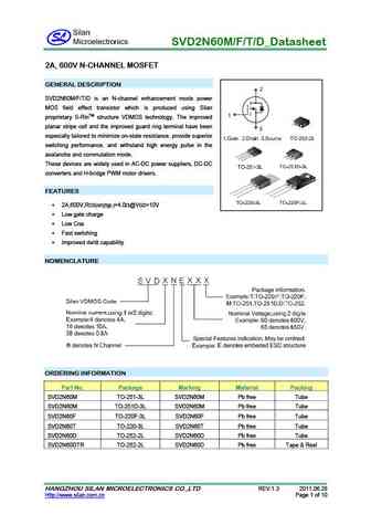
SVD2N60M/F/T/D_Datasheet 2A, 600V N-CHANNEL MOSFET GENERAL DESCRIPTION SVD2N60M/F/T/D is an N-channel enhancement mode power MOS field effect transistor which is produced using Silan proprietary S-RinTM structure VDMOS technology. The improved planar stripe cell and the improved guard ring terminal have been especially tailored to minimize on-state resistance, provide superior s
0.13. Size:746K magnachip
mdd2n60rh mdi2n60.pdf
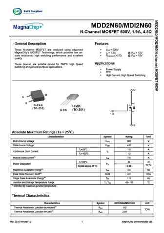
MDD2N60/MDI2N60 N-Channel MOSFET 600V, 1.9A, 4.5 General Description Features These N-channel MOSFET are produced using advanced V = 600V DS MagnaChip s MOSFET Technology, which provides low on- I = 1.9A @ V = 10V D GS state resistance, high switching performance and excellent R 4.5 @ V = 10V DS(ON) GS quality. Applications These devices are suitable device for
0.14. Size:758K bruckewell
msd2n60.pdf
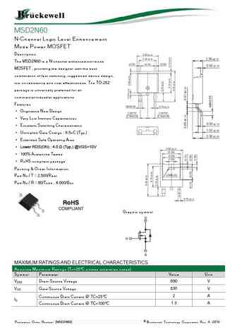
MSD2N60 N-Channel Logic Level Enhancement Mode Power MOSFET Description The MSD2N60 is a N-channel enhancement-mode MOSFET , providing the designer with the best combination of fast switching, ruggedized device design, low on-resistance and cost effectiveness. The TO-252 package is universally preferred for all commercial-industrial applications Features Originative Ne
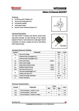
0.15. Size:495K winsemi
wfd2n60.pdf
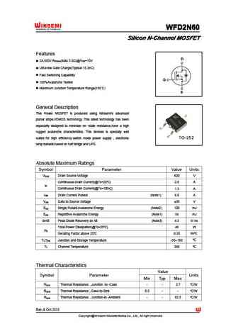
WFD2N60 WFD2N60 WFD2N60 WFD2N60 Silicon N-Channel MOSFET Silicon N-Channel MOSFET Silicon N-Channel MOSFET Silicon N-Channel MOSFET Features 2A,600V,R (Max 5.0 )@V =10V DS(on) GS Ultra-low Gate Charge(Typical 15.3nC) Fast Switching Capability 100%Avalanche Tested Maximum Junction Temperature Range(150 ) General Description This Power MOSFET is produced us
0.16. Size:586K winsemi
wfd2n60b.pdf
WFD2N60B WFD2N60B WFD2N60B WFD2N60B Silicon N-Channel MOSFET Silicon N-Channel MOSFET Silicon N-Channel MOSFET Silicon N-Channel MOSFET Features 2A,600V,R (Max 5.0 )@V =10V DS(on) GS Ultra-low Gate Charge(Typical 9nC) Fast Switching Capability 100%Avalanche Tested Maximum Junction Temperature Range(150 ) General Description This Power MOSFET is produced u
0.17. Size:978K feihonltd
fhf2n60e fhp2n60e fhu2n60e fhd2n60e.pdf
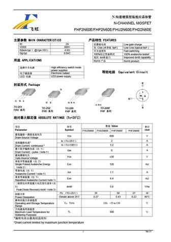
N N-CHANNEL MOSFET FHF2N60E/FHP2N60E/FHU2N60E/FHD2N60E MAIN CHARACTERISTICS FEATURES ID 2A Low gate charge VDSS 600V Crss ( 6pF) Low Crss (typical 6pF ) Rdson-typ @Vgs=10V 4.0 Fast switching Qg-typ 8.0nC 100% 100% avalanche tested dv/
0.18. Size:964K feihonltd
fhf2n60a fhp2n60a fhu2n60a fhd2n60a.pdf
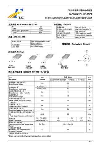
N N-CHANNEL MOSFET FHF2N60A/FHP2N60A/FHU2N60A/FHD2N60A MAIN CHARACTERISTICS FEATURES ID 2A Low gate charge VDSS 600V Crss ( 6pF) Low Crss (typical 6pF ) Rdson-typ @Vgs=10V 3.5 Fast switching Qg-typ 8.0nC 100% 100% avalanche tested dv/
0.19. Size:576K samwin
swd2n60dc swi2n60dc.pdf
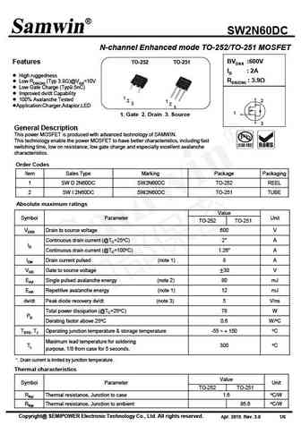
SW2N60DC N-channel Enhanced mode TO-252/TO-251 MOSFET BVDSS 600V Features TO-252 TO-251 ID 2A High ruggedness RDS(ON) 3.9 Low RDS(ON) (Typ 3.9 )@VGS=10V Low Gate Charge (Typ9.5nC) Improved dv/dt Capability 1 100% Avalanche Tested 2 2 1 3 2 Application Charger,Adaptor,LED 3 1 1. Gate 2. Drain 3. Source 3 General Descripti
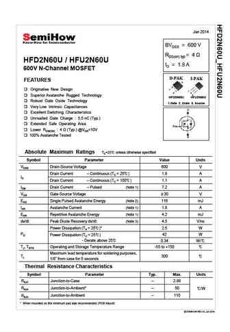
0.20. Size:381K semihow
hfd2n60u hfu2n60u.pdf

June 2015 BVDSS = 600 V RDS(on) typ = 4 HFD2N60U / HFU2N60U ID = 1.8 A 600V N-Channel MOSFET D-PAK I-PAK FEATURES 2 1 Originative New Design 1 3 2 3 Superior Avalanche Rugged Technology HFD2N60U HFU2N60U Robust Gate Oxide Technology 1.Gate 2. Drain 3. Source Very Low Intrinsic Capacitances Excellent Switching Characteristics Unrivalled Gate Charge 5.5 nC (T
0.21. Size:199K semihow
hfd2n60u.pdf
Jan 2014 BVDSS = 600 V RDS(on) typ = 4 HFD2N60U / HFU2N60U ID = 1.8 A 600V N-Channel MOSFET D-PAK I-PAK FEATURES 2 1 Originative New Design 1 3 2 3 Superior Avalanche Rugged Technology HFD2N60U HFU2N60U Robust Gate Oxide Technology 1.Gate 2. Drain 3. Source Very Low Intrinsic Capacitances Excellent Switching Characteristics Unrivalled Gate Charge 5.5 nC (Ty
0.22. Size:160K semihow
hfd2n60s.pdf

March 2014 BVDSS = 600 V RDS(on) typ HFD2N60S / HFU2N60S ID = 1.9 A 600V N-Channel MOSFET D-PAK I-PAK 2 FEATURES 1 1 3 2 3 Originative New Design HFD2N60S HFU2N60S Superior Avalanche Rugged Technology 1.Gate 2. Drain 3. Source Robust Gate Oxide Technology Very Low Intrinsic Capacitances Excellent Switching Characteristics Unrivalled Gate Charge 6.0 nC
0.23. Size:155K semihow
hfd2n60.pdf
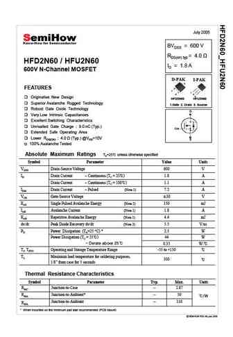
July 2005 BVDSS = 600 V RDS(on) typ HFD2N60 / HFU2N60 ID = 1.8 A 600V N-Channel MOSFET D-PAK I-PAK 2 FEATURES 1 1 3 2 3 Originative New Design HFD2N60 HFU2N60 Superior Avalanche Rugged Technology 1.Gate 2. Drain 3. Source Robust Gate Oxide Technology Very Low Intrinsic Capacitances Excellent Switching Characteristics Unrivalled Gate Charge 9.0 nC (Typ
0.24. Size:514K semihow
hfu2n60f hfd2n60f.pdf
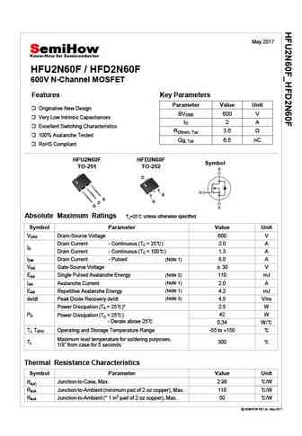
May 2017 HFU2N60F / HFD2N60F 600V N-Channel MOSFET Features Key Parameters Parameter Value Unit Originative New Design BVDSS 600 V Very Low Intrinsic Capacitances ID 2 A Excellent Switching Characteristics RDS(on), Typ 3.6 100% Avalanche Tested Qg, Typ 6.5 nC RoHS Compliant HFU2N60F HFD2N60F Symbol TO-251 TO-252 D S S G D G Ab
0.25. Size:230K semihow
hfd2n60s hfu2n60s.pdf
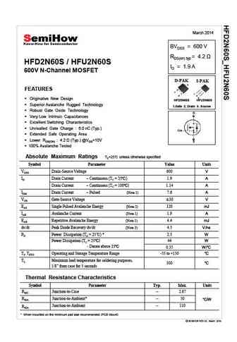
March 2014 BVDSS = 600 V RDS(on) typ HFD2N60S / HFU2N60S ID = 1.9 A 600V N-Channel MOSFET D-PAK I-PAK 2 FEATURES 1 1 3 2 3 Originative New Design HFD2N60S HFU2N60S Superior Avalanche Rugged Technology 1.Gate 2. Drain 3. Source Robust Gate Oxide Technology Very Low Intrinsic Capacitances Excellent Switching Characteristics Unrivalled Gate Charge 6.0 nC
0.26. Size:474K trinnotech
tmd2n60z tmu2n60z.pdf
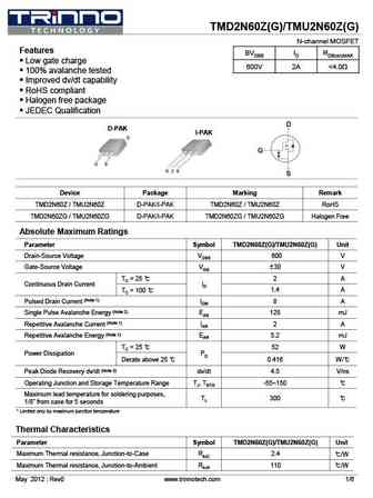
TMD2N60Z(G)/TMU2N60Z(G) N-channel MOSFET Features BVDSS ID RDS(on)MAX Low gate charge 600V 2A
0.27. Size:455K trinnotech
tmd2n60az tmu2n60az.pdf
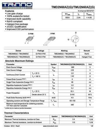
TMD2N60AZ(G)/TMU2N60AZ(G) N-channel MOSFET Features Low gate charge BVDSS ID RDS(on) 100% avalanche tested 600V 2.0A
0.29. Size:1336K lonten
lnd2n60 lnc2n60 lng2n60 lnh2n60.pdf

LND2N60/LNC2N60/LNG2N60/LNH2N60 Lonten N-channel 600V, 2A Power MOSFET Description Product Summary The Power MOSFET is fabricated using the V 600V DSS advanced planer VDMOS technology. The I 2A D resulting device has low conduction resistance, R 4.5 DS(on),max superior switching performance and high avalance Q 10.2 nC g,typ energy. Features Low R DS(on) Low gate charge
0.30. Size:804K cn vbsemi
fqd2n60c.pdf
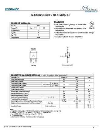
FQD2N60C www.VBsemi.tw N-Channel 650 V (D-S) MOSFET FEATURES PRODUCT SUMMARY Low Gate Charge Qg Results in Simple Drive VDS (V) 650 Available Requirement RDS(on) ( )VGS = 10 V 3.8 RoHS Improved Gate, Avalanche and Dynamic dV/dt Qg (Max.) (nC) 15 Ruggedness Qgs (nC) 3 Fully Characterized Capacitance and Avalanche Voltage and Current Qgd (nC) 6 Compliant to RoHS
0.31. Size:640K cn wuxi unigroup
tma2n60h tmd2n60h tmt2n60h tmu2n60h.pdf
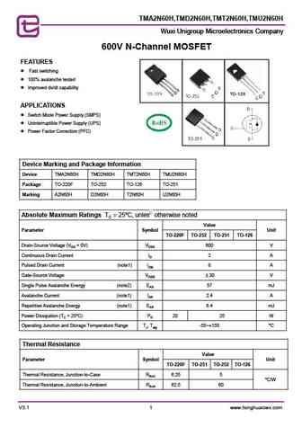
TMA2N60H,TMD2N60H,TMT2N60H,TMU2N60H Wuxi Unigroup Microelectronics Company Wuxi Unigroup Microelectronics Company 600V N-Channel MOSFET FEATURES Fast switching 100% avalanche tested Improved dv/dt capability APPLICATIONS Switch Mode Power Supply (SMPS) Uninterruptible Power Supply (UPS) Power Factor Correction (PFC) Device Marking and Package Info
0.32. Size:265K inchange semiconductor
aod2n60.pdf
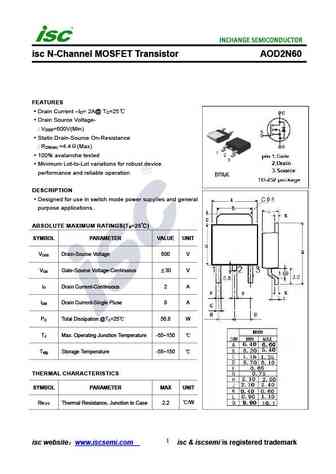
isc N-Channel MOSFET Transistor AOD2N60 FEATURES Drain Current I = 2A@ T =25 D C Drain Source Voltage- V =600V(Min) DSS Static Drain-Source On-Resistance R =4.4 (Max) DS(on) 100% avalanche tested Minimum Lot-to-Lot variations for robust device performance and reliable operation DESCRIPTION Designed for use in switch mode power supplies and general purpose a
0.33. Size:265K inchange semiconductor
aod2n60a.pdf
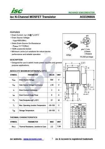
isc N-Channel MOSFET Transistor AOD2N60A FEATURES Drain Current I = 2A@ T =25 D C Drain Source Voltage- V =600V(Min) DSS Static Drain-Source On-Resistance R =4.7 (Max) DS(on) 100% avalanche tested Minimum Lot-to-Lot variations for robust device performance and reliable operation DESCRIPTION Designed for use in switch mode power supplies and general purpose
Otros transistores... FXN0204CQ
, FXN100S55T
, FXN9N20C
, 630
, 110N04
, 13N90
, 14N65
, 18N50D
, STP80NF70
, D4N70
, D4N80
, D50N06
, D5N50
, DH0159
, DH0159B
, DH0159D
, DH0159E
.