B50N06 Datasheet. Equivalente. Reemplazo. Hoja de especificaciones. Principales características
Número de Parte: B50N06 📄📄
Tipo de FET: MOSFET
Polaridad de transistor: N
ESPECIFICACIONES MÁXIMAS
Pdⓘ - Máxima disipación de potencia: 110 W
|Vds|ⓘ - Voltaje máximo drenador-fuente: 68 V
|Vgs|ⓘ - Voltaje máximo fuente-puerta: 20 V
|Id|ⓘ - Corriente continua de drenaje: 60 A
Tjⓘ - Temperatura máxima de unión: 175 °C
CARACTERÍSTICAS ELÉCTRICAS
trⓘ - Tiempo de subida: 100 nS
Cossⓘ - Capacitancia de salida: 174 pF
RDSonⓘ - Resistencia estado encendido drenaje a fuente: 0.015 Ohm
Encapsulados: TO251
📄📄 Copiar
Búsqueda de reemplazo de B50N06 MOSFET
- Selecciónⓘ de transistores por parámetros
B50N06 datasheet
..1. Size:1133K cn wxdh
50n06 f50n06 i50n06 e50n06 b50n06 d50n06.pdf 
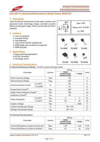
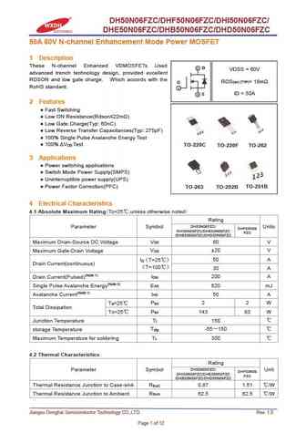
50N06/F50N06/I50N06/ E50N06/B50N06/D50N06 60A 68V N-channel Enhancement Mode Power MOSFET 1 Description These N-channel enhancement mode power mosfets used 2 D V = 68V DSS advanced trench technology design, provided excellent Rdson and low gate charge. Which accords with the RoHS G R = 10.5m DS(on) (TYP) standard. 1 3 S I = 60A D 2 Features Low on resistance Low ga
0.1. Size:289K motorola
mtb50n06vrev3.pdf

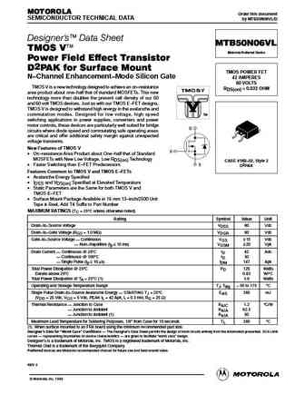
MOTOROLA Order this document SEMICONDUCTOR TECHNICAL DATA by MTB50N06V/D Designer's Data Sheet MTB50N06V TMOS V Motorola Preferred Device Power Field Effect Transistor D2PAK for Surface Mount TMOS POWER FET N Channel Enhancement Mode Silicon Gate 42 AMPERES 60 VOLTS TMOS V is a new technology designed to achieve an on resistance RDS(on) = 0.028 OHM area product about
0.2. Size:91K motorola
mtb50n06el.pdf

MOTOROLA Order this document SEMICONDUCTOR TECHNICAL DATA by MTB50N06EL/D Advance Information MTB50N06EL TMOS E-FET. Motorola Preferred Device Power Field Effect Transistors TMOS POWER FET D2PAK for Surface Mount LOGIC LEVEL Logic Level TMOS (L2TMOS ) 50 AMPERES 60 VOLTS N Channel Enhancement Mode Silicon Gate RDS(on) = 0.028 OHM These TMOS Power FETs are designed fo
0.3. Size:217K motorola
mtb50n06vl.pdf

MOTOROLA Order this document SEMICONDUCTOR TECHNICAL DATA by MTB50N06VL/D Designer's Data Sheet MTB50N06VL TMOS V Motorola Preferred Device Power Field Effect Transistor D2PAK for Surface Mount TMOS POWER FET N Channel Enhancement Mode Silicon Gate 42 AMPERES 60 VOLTS TMOS V is a new technology designed to achieve an on resistance RDS(on) = 0.032 OHM area product abou
0.4. Size:248K motorola
mtb50n06v.pdf
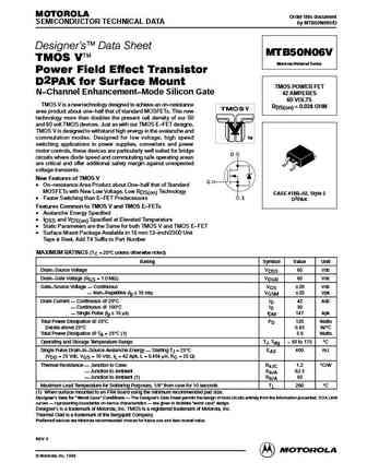
MOTOROLA Order this document SEMICONDUCTOR TECHNICAL DATA by MTB50N06V/D Designer's Data Sheet MTB50N06V TMOS V Motorola Preferred Device Power Field Effect Transistor D2PAK for Surface Mount TMOS POWER FET N Channel Enhancement Mode Silicon Gate 42 AMPERES 60 VOLTS TMOS V is a new technology designed to achieve an on resistance RDS(on) = 0.028 OHM area product about
0.5. Size:97K motorola
mtb50n06elrev1.pdf
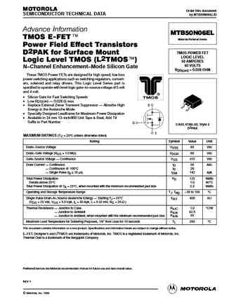
MOTOROLA Order this document SEMICONDUCTOR TECHNICAL DATA by MTB50N06EL/D Advance Information MTB50N06EL TMOS E-FET. Motorola Preferred Device Power Field Effect Transistors TMOS POWER FET D2PAK for Surface Mount LOGIC LEVEL Logic Level TMOS (L2TMOS ) 50 AMPERES 60 VOLTS N Channel Enhancement Mode Silicon Gate RDS(on) = 0.028 OHM These TMOS Power FETs are designed fo
0.6. Size:249K motorola
mtb50n06vlrev2.pdf
MOTOROLA Order this document SEMICONDUCTOR TECHNICAL DATA by MTB50N06VL/D Designer's Data Sheet MTB50N06VL TMOS V Motorola Preferred Device Power Field Effect Transistor D2PAK for Surface Mount TMOS POWER FET N Channel Enhancement Mode Silicon Gate 42 AMPERES 60 VOLTS TMOS V is a new technology designed to achieve an on resistance RDS(on) = 0.032 OHM area product abou
0.7. Size:56K philips
phb50n06t 1.pdf
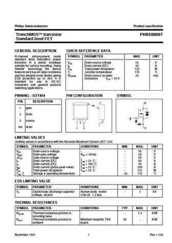
Philips Semiconductors Product specification TrenchMOS transistor PHB50N06T Standard level FET GENERAL DESCRIPTION QUICK REFERENCE DATA N-channel enhancement mode SYMBOL PARAMETER MAX. UNIT standard level field-effect power transistor in a plastic envelope VDS Drain-source voltage 55 V suitable for surface mounting. Using ID Drain current (DC) 50 A trench technology the devic
0.8. Size:55K philips
phb50n06lt.pdf
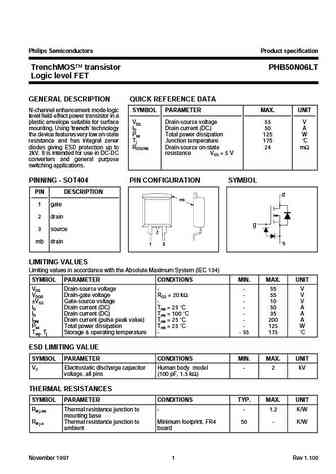
Philips Semiconductors Product specification TrenchMOS transistor PHB50N06LT Logic level FET GENERAL DESCRIPTION QUICK REFERENCE DATA N-channel enhancement mode logic SYMBOL PARAMETER MAX. UNIT level field-effect power transistor in a plastic envelope suitable for surface VDS Drain-source voltage 55 V mounting. Using trench technology ID Drain current (DC) 50 A the device fea
0.9. Size:1038K fairchild semi
fqb50n06 fqi50n06.pdf

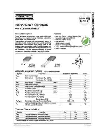
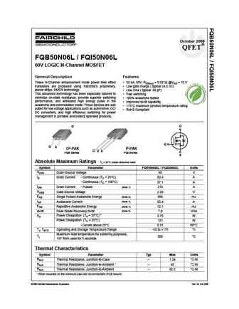
October 2008 QFET FQB50N06 / FQI50N06 60V N-Channel MOSFET General Description Features These N-Channel enhancement mode power field effect 50A, 60V, RDS(on) = 0.022 @VGS = 10 V transistors are produced using Fairchild s proprietary, Low gate charge ( typical 31 nC) planar stripe, DMOS technology. Low Crss ( typical 65 pF) This advanced technology has been especially
0.10. Size:1015K fairchild semi
fqb50n06tm fqi50n06tu.pdf
October 2008 QFET FQB50N06 / FQI50N06 60V N-Channel MOSFET General Description Features These N-Channel enhancement mode power field effect 50A, 60V, RDS(on) = 0.022 @VGS = 10 V transistors are produced using Fairchild s proprietary, Low gate charge ( typical 31 nC) planar stripe, DMOS technology. Low Crss ( typical 65 pF) This advanced technology has been especially
0.11. Size:1022K fairchild semi
fqb50n06ltm fqi50n06ltu.pdf
October 2008 QFET FQB50N06L / FQI50N06L 60V LOGIC N-Channel MOSFET General Description Features These N-Channel enhancement mode power field effect 52.4A, 60V, RDS(on) = 0.021 @VGS = 10 V transistors are produced using Fairchild s proprietary, Low gate charge ( typical 24.5 nC) planar stripe, DMOS technology. Low Crss ( typical 90 pF) This advanced technology has bee
0.12. Size:1052K fairchild semi
fqb50n06l fqi50n06l.pdf

October 2008 QFET FQB50N06L / FQI50N06L 60V LOGIC N-Channel MOSFET General Description Features These N-Channel enhancement mode power field effect 52.4A, 60V, RDS(on) = 0.021 @VGS = 10 V transistors are produced using Fairchild s proprietary, Low gate charge ( typical 24.5 nC) planar stripe, DMOS technology. Low Crss ( typical 90 pF) This advanced technology has bee
0.13. Size:1062K onsemi
fqb50n06 fqi50n06.pdf

Is Now Part of To learn more about ON Semiconductor, please visit our website at www.onsemi.com Please note As part of the Fairchild Semiconductor integration, some of the Fairchild orderable part numbers will need to change in order to meet ON Semiconductor s system requirements. Since the ON Semiconductor product management systems do not have the ability to manage part nomenclatur
0.14. Size:370K cet
cep50n06 ceb50n06.pdf
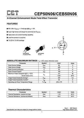
CEP50N06/CEB50N06 N-Channel Enhancement Mode Field Effect Transistor FEATURES 60V, 50A ,RDS(ON) = 17m (typ) @VGS = 10V. Super high dense cell design for extremely low RDS(ON). High power and current handing capability. D Lead free product is acquired. TO-220 & TO-263 package. G CEB SERIES CEP SERIES S TO-263(DD-PAK) TO-220 ABSOLUTE MAXIMUM RATINGS Tc = 25 C unless otherwise no
0.15. Size:756K blue-rocket-elect
brb50n06.pdf
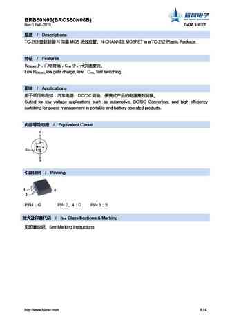
BRB50N06(BRCS50N06B) Rev.C Feb.-2015 DATA SHEET / Descriptions TO-263 N MOS N-CHANNEL MOSFET in a TO-252 Plastic Package. / Features R C DS(on) rss Low RDS(on),low gate charge, low Crss, fast switching. / Applications DC/DC
0.17. Size:840K cn vbsemi
vbzfb50n06.pdf
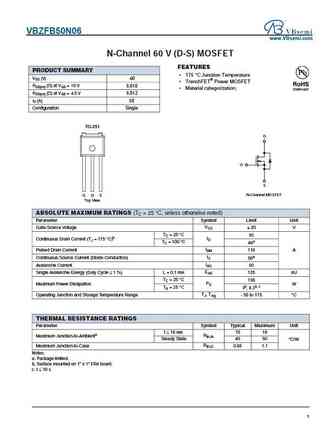
VBZFB50N06 www.VBsemi.com N-Channel 60 V (D-S) MOSFET FEATURES PRODUCT SUMMARY 175 C Junction Temperature VDS (V) 60 TrenchFET Power MOSFET RDS(on) ( ) at VGS = 10 V 0.010 Material categorization RDS(on) ( ) at VGS = 4.5 V 0.012 ID (A) 50 Configuration Single TO-251 D G S N-Channel MOSFET G D S Top View ABSOLUTE MAXIMUM RATINGS (TC = 25 C, unless other
0.18. Size:819K cn vbsemi
fqb50n06.pdf
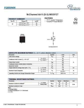
FQB50N06 www.VBsemi.tw N-Channel 60-V (D-S) MOSFET FEATURES PRODUCT SUMMARY 175 C Junction Temperature VDS (V) RDS(on) ( ) ID (A)a TrenchFET Power MOSFET 0.012 at VGS = 10 V 60 60 0.013 at VGS = 4.5 V 50 D D2PAK (TO-263) G G D S S N-Channel MOSFET ABSOLUTE MAXIMUM RATINGS (TC = 25 C, unless otherwise noted) Parameter Symbol Limit Unit VGS Gate-Source
Otros transistores... DH020N03B, DH020N03D, DH020N03E, B25N10, B2N65, B4N60, B4N65, B4N80, AOD4184A, B5N50, B5N65, B630, B640, B740, B7N70, B80N06, DATD063N06N