D630 MOSFET Equivalente. Reemplazo. Hoja de especificaciones. Principales características
Número de Parte: D630
Tipo de FET: MOSFET
Polaridad de transistor: N
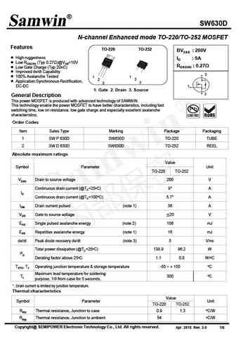
ESPECIFICACIONES MÁXIMAS
Pdⓘ - Máxima disipación de potencia: 75 W
|Vds|ⓘ - Voltaje máximo drenador-fuente: 200 V
|Vgs|ⓘ - Voltaje máximo fuente-puerta: 30 V
|Id|ⓘ - Corriente continua de drenaje: 9 A
Tjⓘ - Temperatura máxima de unión: 150 °C
CARACTERÍSTICAS ELÉCTRICAS
trⓘ - Tiempo de subida: 3.5 nS
Cossⓘ - Capacitancia de salida: 94 pF
RDSonⓘ - Resistencia estado encendido drenaje a fuente: 0.28 Ohm
Encapsulados: TO252
Búsqueda de reemplazo de D630 MOSFET
- Selecciónⓘ de transistores por parámetros
D630 datasheet
630 f630 i630 e630 b630 d630.pdf
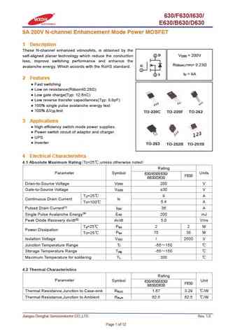
630/F630/I630/ E630/B630/D630 9A 200V N-channel Enhancement Mode Power MOSFET 1 Description These N-channel enhanced vdmosfets, is obtained by the 2 D V = 200V self-aligned planar technology which reduce the conduction DSS loss, improve switching performance and enhance the R = 0.23 DS(on) (TYP) G avalanche energy. Which accords with the RoHS standard. 1 I = 9A 3 S D 2 Feature
fqd630tf fqd630tm.pdf
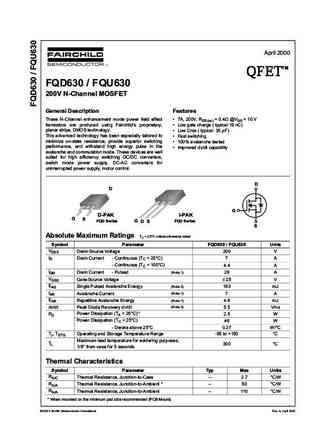
April 2000 TM QFET QFET QFET QFET 200V N-ChanneI MOSFET GeneraI Description Features These N-Channel enhancement mode power field effect 7A, 200V, RDS(on) = 0.4 @VGS = 10 V transistors are produced using Fairchild s proprietary, Low gate charge ( typical 19 nC) planar stripe, DMOS technology. Low Crss ( typical 35 pF) This advanced technology has b
nimd6302r2.pdf
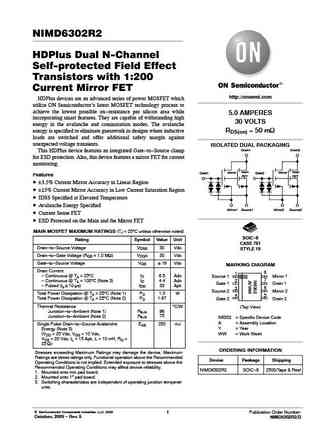
NIMD6302R2 HDPlus Dual N-Channel Self-protected Field Effect Transistors with 1 200 Current Mirror FET http //onsemi.com HDPlus devices are an advanced series of power MOSFET which utilize ON Semiconductor s latest MOSFET technology process to achieve the lowest possible on-resistance per silicon area while 5.0 AMPERES incorporating smart features. They are capable of withstanding h
ceu630n ced630n.pdf
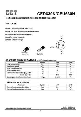
CED630N/CEU630N N-Channel Enhancement Mode Field Effect Transistor FEATURES 200V, 7.5A, RDS(ON) = 0.36 @VGS = 10V. Super high dense cell design for extremely low RDS(ON). High power and current handing capability. D Lead free product is acquired. TO-251 & TO-252 package. D G G S CEU SERIES CED SERIES S TO-252(D-PAK) TO-251(I-PAK) ABSOLUTE MAXIMUM RATINGS Tc = 25 C unless oth

Otros transistores... DH009N02I, DH009N02P, DH012N03, DH012N03B, D12N06, D18N20, D25N10, D5N65-XAD, 2N7000, D640, D740, D7N60, D7N70, D80N06, D8N50, D9N65, 18P10
🌐 : EN ES РУ

Liste
Recientemente añadidas las descripciónes de los transistores:
MOSFET: AUW033N08BG | AUW025N10 | AUR030N10 | AUR020N10 | AUR020N085 | AUR014N10 | AUP074N10 | AUP065N10 | AUP062N08BG | AUP060N08AG | HYG053N10NS1B | HYG053N10NS1P | AP220N04T | AP220N04P | QM3126M3 | AUP060N055
Popular searches
2sd1047 transistor | mj802 | bu508a | bc560c | ksa1220ay | irf 830 | mpsa56 transistor | transistor 2222a