ASDM30P100KQ Datasheet. Equivalente. Reemplazo. Hoja de especificaciones. Principales características
Número de Parte: ASDM30P100KQ 📄📄
Tipo de FET: MOSFET
Polaridad de transistor: P
ESPECIFICACIONES MÁXIMAS
Pdⓘ - Máxima disipación de potencia: 109 W
|Vds|ⓘ - Voltaje máximo drenador-fuente: 30 V
|Vgs|ⓘ - Voltaje máximo fuente-puerta: 20 V
|Id|ⓘ - Corriente continua de drenaje: 100 A
Tjⓘ - Temperatura máxima de unión: 175 °C
CARACTERÍSTICAS ELÉCTRICAS
trⓘ - Tiempo de subida: 13 nS
Cossⓘ - Capacitancia de salida: 742 pF
RDSonⓘ - Resistencia estado encendido drenaje a fuente: 0.006 Ohm
Encapsulados: TO252
Búsqueda de reemplazo de ASDM30P100KQ MOSFET
- Selecciónⓘ de transistores por parámetros
ASDM30P100KQ datasheet
asdm30p100kq.pdf
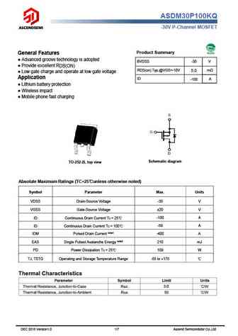
ASDM30P100KQ -30V P-Channel MOSFET Product Summary General Features Advanced groove technology is adopted BVDSS -30 V Provide excellent R DS(ON) RDS(on).Typ.@VGS=-10V m 5.0 Low gate charge and operate at low gate voltage Application ID -100 A Lithium battery protection Wireless impact Mobile phone fast charging Schematic diagram TO-252-2L top view
asdm30p11td-r.pdf
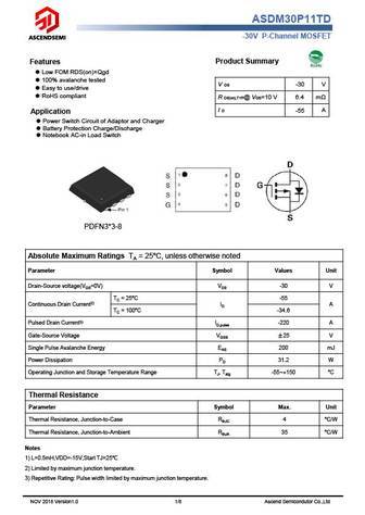
ASDM30P11TD -30V P-Channel MOSFET Product Summary Features Low FOM RDS(on) Qgd 100% avalanche tested V DS -30 V Easy to use/drive RoHS compliant R DS(on),TYP@ VGS=10 V 6.4 m I D -55 A Application Power Switch Circuit of Adaptor and Charger Battery Protection Charge/Discharge Notebook AC-in Load Switch PDFN3*3-8 Absolute Maximum Ratings TA = 25 u
asdm30p11td.pdf
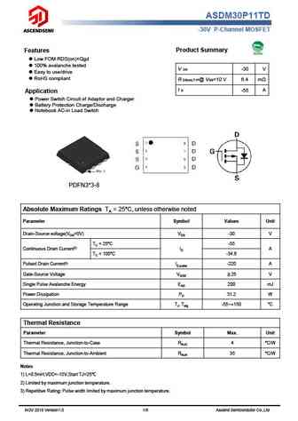
ASDM30P11TD -30V P-Channel MOSFET Product Summary Features Low FOM RDS(on) Qgd 100% avalanche tested V DS -30 V Easy to use/drive RoHS compliant R DS(on),TYP@ VGS=10 V 6.4 m I D -55 A Application Power Switch Circuit of Adaptor and Charger Battery Protection Charge/Discharge Notebook AC-in Load Switch PDFN3*3-8 Absolute Maximum Ratings TA = 25 u
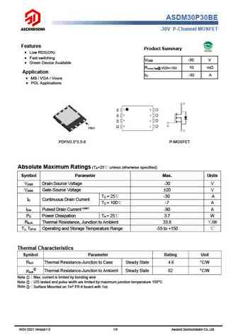
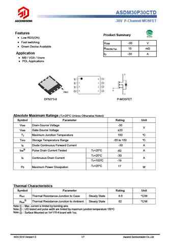
asdm30p30ctd-r.pdf

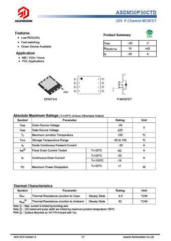
ASDM30P30CTD -30V P-Channel MOSFET Features Product Summary Low RDS(ON) Fast switching V -30 V DSS Green Device Available R 15 m DS(ON)-Typ. Application I -30 A D MB / VGA / Vcore POL Applications DFN3*3-8 P-MOSFET Absolute Maximum Ratings (T =25 C Unless Otherwise Noted) J Symbol Parameter Rating Unit VDSS Drain-Source Voltage -30 V VGSS Gate-
Otros transistores... ASDM30DN30E, ASDM30DN40E, ASDM30N100KQ, ASDM30N120KQ, ASDM30N120Q, ASDM30N150Q, ASDM30N75KQ, ASDM30N90Q, AO3400A
🌐 : EN ES РУ

Liste
Recientemente añadidas las descripciónes de los transistores:
MOSFET: ASDM30P100KQ | ASDM30N90Q | ASDM30N75KQ | ASDM30N150Q | ASDM30N120Q | ASDM30N120KQ | ASDM30N100KQ | ASDM30DN40E | ASDM30DN30E | ASDM3050KQ | ASDM2305 | ASDM2301 | ASDM2300ZA | ASDM20P13S | ASDM20N90Q | ASDM20N60
Popular searches
irfp460 | irfz44n mosfet | lm317t datasheet | irf540 | bc337 | ksc1845 | c1815 transistor | 2sc1815