NTP6410AN MOSFET Equivalente. Reemplazo. Hoja de especificaciones. Principales características
Número de Parte: NTP6410AN
Tipo de FET: MOSFET
Polaridad de transistor: N
ESPECIFICACIONES MÁXIMAS
Pdⓘ - Máxima disipación de potencia: 188 W
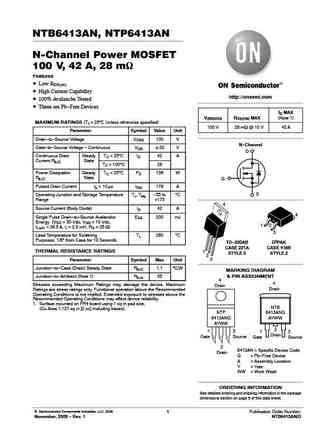
|Vds|ⓘ - Voltaje máximo drenador-fuente: 100 V
|Vgs|ⓘ - Voltaje máximo fuente-puerta: 20 V
|Id|ⓘ - Corriente continua de drenaje: 76 A
Tjⓘ - Temperatura máxima de unión: 175 °C
CARACTERÍSTICAS ELÉCTRICAS
trⓘ - Tiempo de subida: 170 nS
Cossⓘ - Capacitancia de salida: 650 pF
RDSonⓘ - Resistencia estado encendido drenaje a fuente: 0.012 Ohm
Encapsulados: TO220AB
Búsqueda de reemplazo de NTP6410AN MOSFET
- Selecciónⓘ de transistores por parámetros
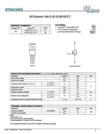
NTP6410AN datasheet
ntb6410an ntp6410an.pdf
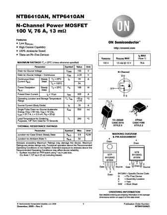
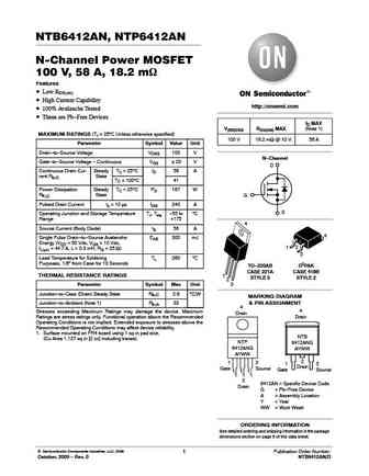
NTB6410AN, NTP6410AN N-Channel Power MOSFET 100 V, 76 A, 13 mW Features Low RDS(on) High Current Capability http //onsemi.com 100% Avalanche Tested These are Pb-Free Devices ID MAX V(BR)DSS RDS(ON) MAX (Note 1) MAXIMUM RATINGS (TJ = 25 C Unless otherwise specified) 100 V 13 mW @ 10 V 76 A Parameter Symbol Value Unit Drain-to-Source Voltage VDSS 100 V N-Channel G
ntb6410an ntp6410an nvb6410an.pdf
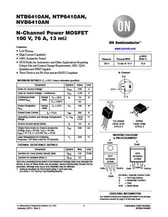
NTB6410AN, NTP6410AN, NVB6410AN N-Channel Power MOSFET 100 V, 76 A, 13 mW Features www.onsemi.com Low RDS(on) High Current Capability ID MAX 100% Avalanche Tested V(BR)DSS RDS(ON) MAX (Note 1) NVB Prefix for Automotive and Other Applications Requiring 100 V 13 mW @ 10 V 76 A Unique Site and Control Change Requirements; AEC-Q101 Qualified and PPAP Capable N-Channel
ntb6410ang ntp6410ang.pdf
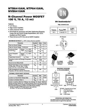
NTB6410AN, NTP6410AN, NVB6410AN N-Channel Power MOSFET 100 V, 76 A, 13 mW Features http //onsemi.com Low RDS(on) High Current Capability ID MAX 100% Avalanche Tested V(BR)DSS RDS(ON) MAX (Note 1) NVB Prefix for Automotive and Other Applications Requiring 100 V 13 mW @ 10 V 76 A Unique Site and Control Change Requirements; AEC-Q101 Qualified and PPAP Capable N-Chan
ntb6412ang ntp6412ang.pdf
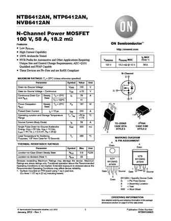
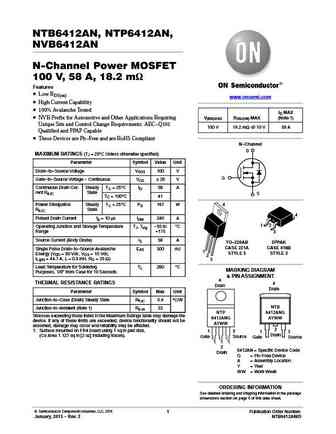
NTB6412AN, NTP6412AN, NVB6412AN N-Channel Power MOSFET 100 V, 58 A, 18.2 mW Features Low RDS(on) http //onsemi.com High Current Capability 100% Avalanche Tested ID MAX NVB Prefix for Automotive and Other Applications Requiring V(BR)DSS RDS(ON) MAX (Note 1) Unique Site and Control Change Requirements; AEC-Q101 100 V 18.2 mW @ 10 V 58 A Qualified and PPAP Capable


Otros transistores... NTMS5838NL , NTMS5P02 , NTMS7N03R2 , NTNUS3171PZ , NTP2955 , NTP5404N , NTP5863N , NTP5864N , 2SK3878 , NTP6411AN , NTP6412AN , NTP6413AN , NTR0202PL , NTR1P02 , NTR1P02LT1 , NTR2101P , NTR4003N .
History: 2SJ292 | BSS214NW
🌐 : EN ES РУ

Liste
Recientemente añadidas las descripciónes de los transistores:
MOSFET: AUB062N08BG | AUB060N08AG | AUB056N10 | AUB056N08BGL | AUB050N085 | AUB050N055 | AUB045N12 | AUB045N10BT | AUB039N10 | AUB034N10 | AUB033N08BG | AUB026N085 | AUA062N08BG | AUA060N08AG | AUA056N08BGL | AUA039N10
Popular searches
2sd2560 | 2sc2078 transistor | bc558 datasheet | p75nf75 mosfet | ao4407a | mpsa06 datasheet | bc548 pinout | bdw94c