cep60n10 ceb60n10.pdf Principales características:
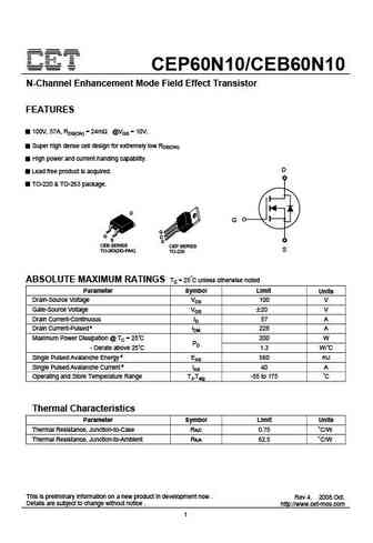
CEP60N10/CEB60N10 N-Channel Enhancement Mode Field Effect Transistor FEATURES 100V, 57A, RDS(ON) = 24m @VGS = 10V. Super high dense cell design for extremely low RDS(ON). High power and current handing capability. D Lead free product is acquired. TO-220 & TO-263 package. G CEB SERIES CEP SERIES S TO-263(DD-PAK) TO-220 ABSOLUTE MAXIMUM RATINGS Tc = 25 C unless otherwise noted Parameter Symbol Limit Units Drain-Source Voltage VDS 100 V Gate-Source Voltage VGS 20 V Drain Current-Continuous ID 57 A Drain Current-Pulsed a IDM 228 A Maximum Power Dissipation @ TC = 25 C 200 W PD - Derate above 25 C 1.3 W/ C Single Pulsed Avalanche Energy d EAS 560 mJ Single Pulsed Avalanche Current d IAS 40 A Operating and Store Temperature Range TJ,Tstg -55 to 175 C Thermal Characteristics Parameter Symbol Limit Units Thermal Resistance, Junction-to-Case R JC 0.75 C/W Th... MOSTRAR MÁS ⇒
Keywords - ALL TRANSISTORS. Principales características
cep60n10 ceb60n10.pdf Design, MOSFET, Power
cep60n10 ceb60n10.pdf RoHS Compliant, Service, Triacs, Semiconductor
cep60n10 ceb60n10.pdf Database, Innovation, IC, Electricity
Parámetros del transistor bipolar y su interrelación.
🌐 : EN ES РУ

Liste
Recientemente añadidas las descripciónes de los transistores:
BJT: ZDT6705 | GA1L4Z | GA1A4M | SBT42 | 2SA200-Y | 2SA200-O | 2SD882-Q | 2SD882-P | 2SD882-E | 2SC945-L | 2SC945-H | 2SC4226-R23 | 2SC3357-F | 2SC3357-E | 2SC3356-R26 | 2SC3356-R24 | 2SC3356-R23 | 2SB772-Q | 2SB772-P | 2SB772-E | 2SA1015-L
Popular searches
irfz44n | irf3205 | irfz44n datasheet | 2n4401 | bc547 transistor | bd139 | 2n4401 datasheet