2SD1117 Datasheet. Equivalente. Reemplazo. Hoja de especificaciones. Principales características
Número de Parte: 2SD1117 📄📄
Material: Si
Polaridad de transistor: NPN
ESPECIFICACIONES MÁXIMAS
Disipación total del dispositivo (Pc): 50 W
Tensión colector-base (Vcb): 40 V
Tensión emisor-base (Veb): 7 V
Corriente del colector DC máxima (Ic): 10 A
Temperatura operativa máxima (Tj): 150 °C
CARACTERÍSTICAS ELÉCTRICAS
Ganancia de corriente contínua (hFE): 120
Encapsulados: TO220
📄📄 Copiar
Búsqueda de reemplazo de 2SD1117
- Selecciónⓘ de transistores por parámetros
2SD1117 datasheet
..1. Size:208K inchange semiconductor
2sd1117.pdf 
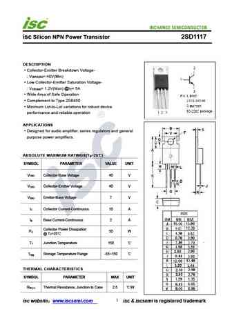
isc Silicon NPN Power Transistor 2SD1117 DESCRIPTION Collector-Emitter Breakdown Voltage- V = 40V(Min) (BR)CEO Low Collector-Emitter Saturation Voltage- V = 1.2V(Max) @I = 5A CE(sat) C Wide Area of Safe Operation Complement to Type 2SB850 Minimum Lot-to-Lot variations for robust device performance and reliable operation APPLICATIONS Designed for audio amplifier, ser
8.1. Size:71K sanyo
2sd1111.pdf
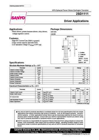
Ordering number EN751C NPN Epitaxial Planar Silicon Darlington Transistor 2SD1111 Driver Applications Applications Package Dimensions Motor drivers, printer hammer drivers, relay drivers, unit mm voltage regulator control. 2003B [2SD1111] 5.0 Features 4.0 4.0 High DC Current Gain (5000 or greater). Large current capacity and wide ASO. Low saturation voltage (VCE(
8.2. Size:42K panasonic
2sd1119 e.pdf
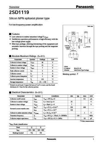
Transistor 2SD1119 Silicon NPN epitaxial planer type For low-frequency power amplification Unit mm 1.5 0.1 4.5 0.1 1.6 0.2 Features Low collector to emitter saturation voltage VCE(sat). Satisfactory operation performances at high efficiency with the 45 low-voltage power supply. Mini type package, allowing downsizing of the equipment and 0.4 0.08 automatic insertion thr
8.3. Size:38K panasonic
2sd1119.pdf

Transistor 2SD1119 Silicon NPN epitaxial planer type For low-frequency power amplification Unit mm 1.5 0.1 4.5 0.1 1.6 0.2 Features Low collector to emitter saturation voltage VCE(sat). Satisfactory operation performances at high efficiency with the 45 low-voltage power supply. Mini type package, allowing downsizing of the equipment and 0.4 0.08 automatic insertion thr
8.4. Size:100K fuji
2sd1118.pdf
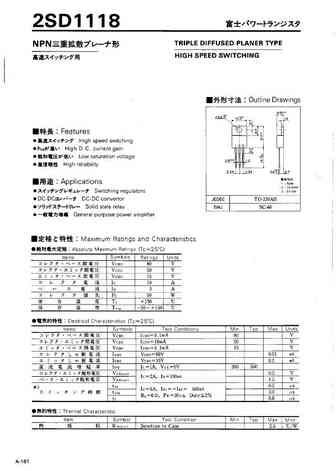
Fuji Semiconductor, Inc. - P.O. Box 702708 - Dallas, TX 75370 - 972-733-1700 - www.fujisemiconductor.com
8.5. Size:32K hitachi
2sd1113.pdf
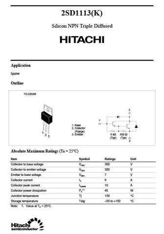
2SD1113(K) Silicon NPN Triple Diffused Application Igniter Outline TO-220AB 2 1 1. Base 2. Collector (Flange) 1 3. Emitter 6 k 450 2 3 (Typ) (Typ) 3 Absolute Maximum Ratings (Ta = 25 C) Item Symbol Ratings Unit Collector to base voltage VCBO 300 V Collector to emitter voltage VCEO 300 V Emitter to base voltage VEBO 7V Collector current IC 6A Collector peak current
8.6. Size:510K htsemi
2sd1119.pdf
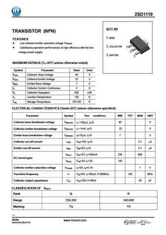
2SD1119 SOT-89 TRANSISTOR (NPN) 1. BASE FEATURES Low collector-emitter saturation voltage VCE(sat) 2. COLLECTOR 1 Satisfactory operation performances at high efficiency with the low 2 voltage power supply. 3. EMITTER 3 MAXIMUM RATINGS (TA=25 unless otherwise noted) Symbol Parameter Value Units VCBO Collector- Base Voltage 40 V VCEO Collector-Emitter Voltage
8.7. Size:187K lge
2sd1119.pdf
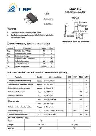
2SD1119 SOT-89 Transistor(NPN) 1. BASE SOT-89 2. COLLECTOR 1 4.6 2 B 4.4 1.6 1.8 3. EMITTER 1.4 3 1.4 2.6 4.25 Features 2.4 3.75 0.8 Low collector-emitter saturation voltage VCE(sat) MIN 0.53 Satisfactory operation performances at high efficiency with the low 0.40 0.48 0.44 2x) 0.13 B 0.35 0.37 1.5 voltage power supply. 3.0 Dimensions in inches a
8.8. Size:299K kexin
2sd1119.pdf
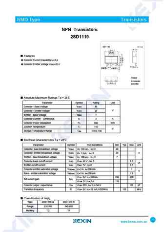
SMD Type Transistors NPN Transistors 2SD1119 1.70 0.1 Features Collector Current Capability IC=3 A Collector Emitter Voltage VCEO=25 V 0.42 0.1 0.46 0.1 1.Base 2.Collector 3.Emitter Absolute Maximum Ratings Ta = 25 Parameter Symbol Rating Unit Collector - Base Voltage VCBO 40 Collector - Emitter Voltage VCEO 25 V Emitter - Base Voltage VEBO 7 Collector
8.9. Size:209K inchange semiconductor
2sd1115.pdf
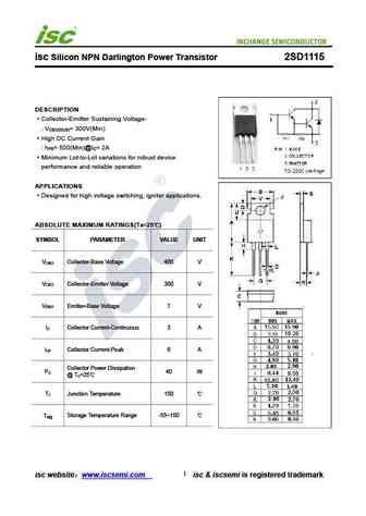
isc Silicon NPN Darlington Power Transistor 2SD1115 DESCRIPTION Collector-Emitter Sustaining Voltage- V = 300V(Min) CEO(SUS) High DC Current Gain h = 500(Min)@I = 2A FE C Minimum Lot-to-Lot variations for robust device performance and reliable operation APPLICATIONS Designed for high voltage switching, igniter applications. ABSOLUTE MAXIMUM RATINGS(T =25 ) a SYMBOL P
8.10. Size:209K inchange semiconductor
2sd1118.pdf
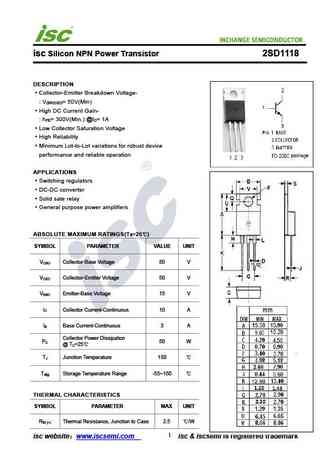
isc Silicon NPN Power Transistor 2SD1118 DESCRIPTION Collector-Emitter Breakdown Voltage- V = 50V(Min) (BR)CEO High DC Current Gain- h = 300V(Min.) @I = 1A FE C Low Collector Saturation Voltage High Reliability Minimum Lot-to-Lot variations for robust device performance and reliable operation APPLICATIONS Switching regulators DC-DC converter Solid sate relay
8.11. Size:186K inchange semiconductor
2sd1114.pdf
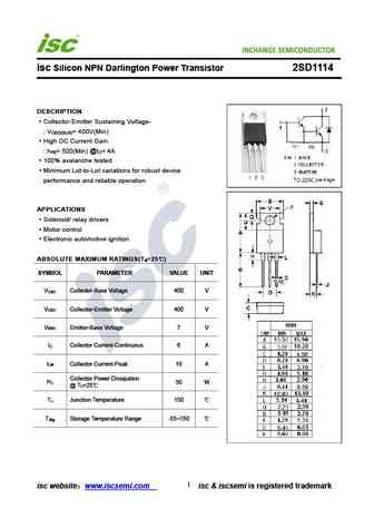
INCHANGE Semiconductor isc Silicon NPN Darlington Power Transistor 2SD1114 DESCRIPTION Collector-Emitter Sustaining Voltage- V = 400V(Min) CEO(SUS) High DC Current Gain h = 500(Min) @I = 4A FE C 100% avalanche tested Minimum Lot-to-Lot variations for robust device performance and reliable operation APPLICATIONS Solenoid/ relay drivers Motor control Electronic au
8.12. Size:57K inchange semiconductor
2sd1115k.pdf
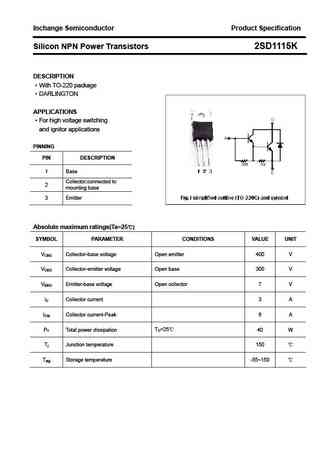
Inchange Semiconductor Product Specification Silicon NPN Power Transistors 2SD1115K DESCRIPTION With TO-220 package DARLINGTON APPLICATIONS For high voltage switching and ignitor applications PINNING PIN DESCRIPTION 1 Base Collector;connected to 2 mounting base 3 Emitter Absolute maximum ratings(Ta=25 ) SYMBOL PARAMETER CONDITIONS VALUE UNIT VCBO Collecto
8.13. Size:217K inchange semiconductor
2sd1110.pdf
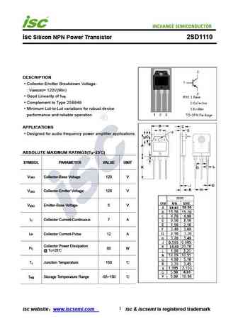
isc Silicon NPN Power Transistor 2SD1110 DESCRIPTION Collector-Emitter Breakdown Voltage- V = 120V(Min) (BR)CEO Good Linearity of h FE Complement to Type 2SB849 Minimum Lot-to-Lot variations for robust device performance and reliable operation APPLICATIONS Designed for audio frequency power amplifier applications. ABSOLUTE MAXIMUM RATINGS(T =25 ) a SYMBOL PARAMETER V
8.14. Size:211K inchange semiconductor
2sd1113.pdf
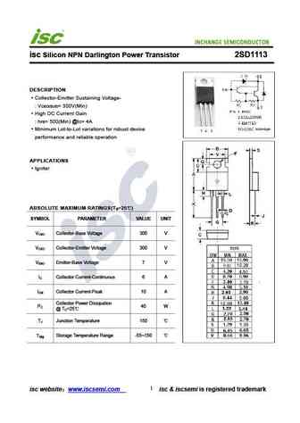
INCHANGE Semiconductor isc Silicon NPN Darlington Power Transistor 2SD1113 DESCRIPTION Collector-Emitter Sustaining Voltage- V = 300V(Min) CEO(SUS) High DC Current Gain h = 500(Min) @I = 4A FE C Minimum Lot-to-Lot variations for robust device performance and reliable operation APPLICATIONS Igniter ABSOLUTE MAXIMUM RATINGS(T =25 ) a SYMBOL PARAMETER VALUE UNIT V Col
8.15. Size:207K inchange semiconductor
2sd111.pdf
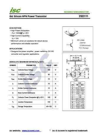
isc Silicon NPN Power Transistor 2SD111 DESCRIPTION High Power Dissipation- P = 100W@T = 25 C C High Current Capability- I = 10A C Minimum Lot-to-Lot variations for robust device performance and reliable operation APPLICATIONS Designed for power amplifier , power switching ,DC-DC converter and regulator applications. ABSOLUTE MAXIMUM RATINGS(T =25 ) a SYMBOL PARA
Otros transistores... 2SD1112, 2SD1113, 2SD1113K, 2SD1114, 2SD1114K, 2SD1115, 2SD1115K, 2SD1116, BC337, 2SD1117A, 2SD1118, 2SD1119, 2SD1120, 2SD1120O, 2SD1121, 2SD1122, 2SD1123
