2N25 Equivalente. Reemplazo. Hoja de especificaciones. Principales características
Número de Parte: 2N25
Material: Ge
Polaridad de transistor: PNP
ESPECIFICACIONES MÁXIMAS
Disipación total del dispositivo (Pc): 0.2 W
Tensión colector-base (Vcb): 50 V
Tensión colector-emisor (Vce): 45 V
Tensión emisor-base (Veb): 12 V
Corriente del colector DC máxima (Ic): 0.03 A
Temperatura operativa máxima (Tj): 90 °C
CARACTERÍSTICAS ELÉCTRICAS
Transición de frecuencia (fT): 9 MHz
Ganancia de corriente contínua (hFE): 22
Encapsulados: TO7
Búsqueda de reemplazo de 2N25
- Selecciónⓘ de transistores por parámetros
2N25 datasheet
..1. Size:1372K goford
2n25.pdf 
GOFORD 2N25 Description Features VDSS RDS(ON) ID @ 10V (typ) 2A 250V 2.2 Fast switching 100% avalanche tested Improved dv/dt capability TO-251 TO-252 Application DC Motor Control and Class D Amplifier Uninterruptible Power Supply (UPS) Automotive Absolute Maximum Ratings TC=25 unless otherwise specified Max. Symbol Parameter U
0.1. Size:267K motorola
mtv32n25e.pdf
MOTOROLA Order this document SEMICONDUCTOR TECHNICAL DATA by MTV32N25E/D Designer's Data Sheet MTV32N25E TMOS E-FET. Power Field Effect Transistor D3PAK for Surface Mount TMOS POWER FET N Channel Enhancement Mode Silicon Gate 32 AMPERES 250 VOLTS The D3PAK package has the capability of housing the largest chip RDS(on) = 0.08 OHM size of any standard, plastic, surface mo
0.2. Size:94K motorola
mtw32n25e.pdf

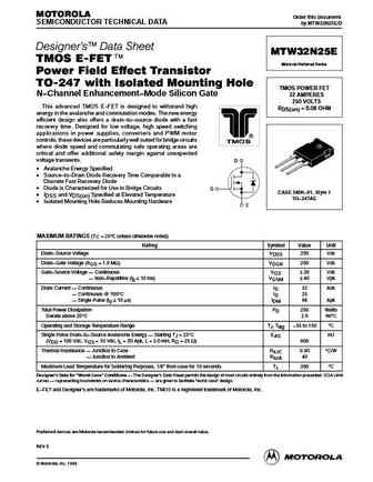
MOTOROLA Order this document SEMICONDUCTOR TECHNICAL DATA by MTW32N25E/D Designer's Data Sheet MTW32N25E TMOS E-FET. Motorola Preferred Device Power Field Effect Transistor TO-247 with Isolated Mounting Hole TMOS POWER FET N Channel Enhancement Mode Silicon Gate 32 AMPERES 250 VOLTS This advanced TMOS E FET is designed to withstand high RDS(on) = 0.08 OHM energy in
0.3. Size:139K motorola
mmft2n25erev0.pdf
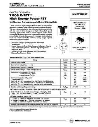
MOTOROLA Order this document SEMICONDUCTOR TECHNICAL DATA by MMFT2N25E/D Product Preview MMFT2N25E TMOS E-FET High Energy Power FET N Channel Enhancement Mode Silicon Gate TMOS POWER FET 2.0 AMPERES This advanced high voltage TMOS E FET is designed to 250 VOLTS withstand high energy in the avalanche mode and switch efficiently. RDS(on) = 3.5 W This new high energy device
0.4. Size:143K motorola
mmft2n25e.pdf

MOTOROLA Order this document SEMICONDUCTOR TECHNICAL DATA by MMFT2N25E/D Product Preview MMFT2N25E TMOS E-FET High Energy Power FET N Channel Enhancement Mode Silicon Gate TMOS POWER FET 2.0 AMPERES This advanced high voltage TMOS E FET is designed to 250 VOLTS withstand high energy in the avalanche mode and switch efficiently. RDS(on) = 3.5 W This new high energy device
0.5. Size:151K motorola
mtw32n25erev2.pdf
MOTOROLA Order this document SEMICONDUCTOR TECHNICAL DATA by MTW32N25E/D Designer's Data Sheet MTW32N25E TMOS E-FET. Motorola Preferred Device Power Field Effect Transistor TO-247 with Isolated Mounting Hole TMOS POWER FET N Channel Enhancement Mode Silicon Gate 32 AMPERES 250 VOLTS This advanced TMOS E FET is designed to withstand high RDS(on) = 0.08 OHM energy in
0.6. Size:109K international rectifier
irfu12n25d.pdf

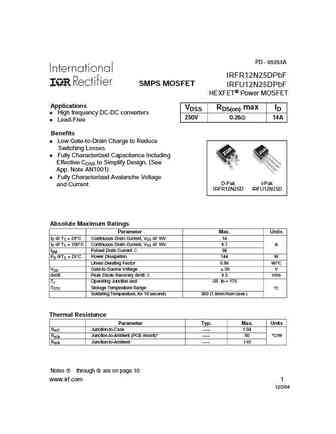
PD - 94296A IRFR12N25D SMPS MOSFET IRFU12N25D HEXFET Power MOSFET Applications VDSS RDS(on) max ID High frequency DC-DC converters 250V 0.26 14A Benefits Low Gate-to-Drain Charge to Reduce Switching Losses Fully Characterized Capacitance Including Effective COSS to Simplify Design, (See App. Note AN1001) Fully Characterized Avalanche Voltage D-Pak I-Pak and Current I
0.7. Size:225K international rectifier
irfr12n25dpbf irfu12n25dpbf.pdf
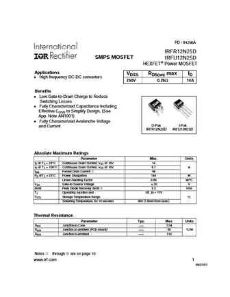
PD - 95353A IRFR12N25DPbF SMPS MOSFET IRFU12N25DPbF HEXFET Power MOSFET Applications VDSS RDS(on) max ID l High frequency DC-DC converters 250V 0.26 14A l Lead-Free Benefits l Low Gate-to-Drain Charge to Reduce Switching Losses l Fully Characterized Capacitance Including Effective COSS to Simplify Design, (See App. Note AN1001) l Fully Characterized Avalanche Voltage D-Pa
0.8. Size:104K international rectifier
irfr12n25d.pdf
PD - 94296A IRFR12N25D SMPS MOSFET IRFU12N25D HEXFET Power MOSFET Applications VDSS RDS(on) max ID High frequency DC-DC converters 250V 0.26 14A Benefits Low Gate-to-Drain Charge to Reduce Switching Losses Fully Characterized Capacitance Including Effective COSS to Simplify Design, (See App. Note AN1001) Fully Characterized Avalanche Voltage D-Pak I-Pak and Current I
0.9. Size:772K st
stl52n25m5.pdf
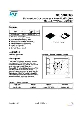
STL52N25M5 N-channel 250 V, 0.055 , 28 A, PowerFLAT (5x6) MDmesh V Power MOSFET Features RDS(on) Type VDSS ID(1) max. STL52N25M5 250 V
0.10. Size:474K st
stp52n25m5.pdf
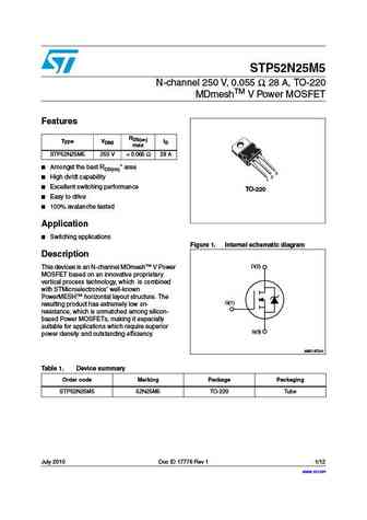
STP52N25M5 N-channel 250 V, 0.055 , 28 A, TO-220 MDmeshTM V Power MOSFET Features RDS(on) Type VDSS ID max STP52N25M5 250 V
0.11. Size:597K fairchild semi
fqa62n25c.pdf
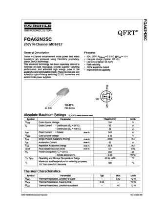
QFET FQA62N25C 250V N-Channel MOSFET General Description Features These N-Channel enhancement mode power field effect 62A, 250V, RDS(on) = 0.035 @VGS = 10 V transistors are produced using Fairchild s proprietary, Low gate charge ( typical 100 nC) planar, DMOS technology. Low Crss ( typical 63.5 pF) This advanced technology has been especially tailored to Fast s
0.13. Size:180K ixys
ixbt2n250.pdf
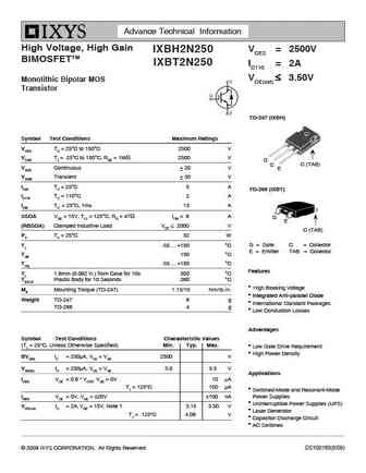
Advance Technical Information High Voltage, High Gain VCES = 2500V IXBH2N250 BIMOSFETTM IXBT2N250 IC110 = 2A VCE(sat) 3.50V Monolithic Bipolar MOS Transistor TO-247 (IXBH) Symbol Test Conditions Maximum Ratings VCES TC = 25 C to 150 C 2500 V VCGR TJ = 25 C to 150 C, RGE = 1M 2500 V G C (TAB) C VGES Continuous 20 V E VGEM Transient 30 V IC
0.14. Size:206K ixys
ixbh42n250.pdf
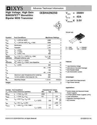
Advance Technical Information High Voltage, High Gain VCES = 2500V IXBH42N250 BIMOSFETTM Monolithic IC110 = 42A Bipolar MOS Transistor VCE(sat) 3.0V TO-247 AD Symbol Test Conditions Maximum Ratings VCES TC = 25 C to 150 C 2500 V G C Tab VCGR TJ = 25 C to 150 C, RGE = 1M 2500 V E VGES Continuous 25 V G = Gate C = Collector VGEM Transient 35
0.15. Size:175K ixys
ixgh2n250.pdf

Advance Technical Information High Voltage IGBTs VCES = 2500V IXGH2N250 IXGT2N250 IC110 = 2A for Capacitor Discharge VCE(sat) 3.1V Applications TO-247 (IXGH) Symbol Test Conditions Maximum Ratings G C (TAB) VCES TC = 25 C to 150 C 2500 V C E VCGR TJ = 25 C to 150 C, RGE = 1M 2500 V VGES Continuous 20 V VGEM Transient 30 V TO-268 (IXGT) IC2
0.16. Size:175K ixys
ixgt2n250.pdf
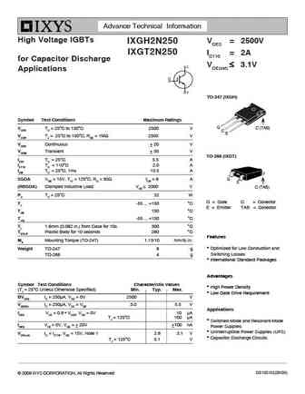
Advance Technical Information High Voltage IGBTs VCES = 2500V IXGH2N250 IXGT2N250 IC110 = 2A for Capacitor Discharge VCE(sat) 3.1V Applications TO-247 (IXGH) Symbol Test Conditions Maximum Ratings G C (TAB) VCES TC = 25 C to 150 C 2500 V C E VCGR TJ = 25 C to 150 C, RGE = 1M 2500 V VGES Continuous 20 V VGEM Transient 30 V TO-268 (IXGT) IC2
0.17. Size:583K ixys
ixtk62n25.pdf
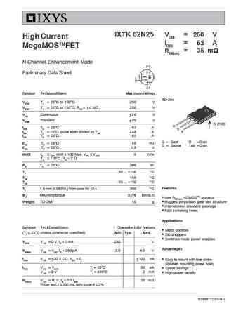
IXTK 62N25 VDSS = 250 V High Current ID25 = 62 A MegaMOSTMFET RDS(on) = 35 m N-Channel Enhancement Mode Preliminary Data Sheet Symbol Test conditions Maximum ratings TO-264 VDSS TJ = 25 C to 150 C 250 V VDGR TJ = 25 C to 150 C; RGS = 1.0 M 250 V VGS Continuous 20 V VGSM Transient 30 V D (TAB) G ID25 TC = 25 C62 A D IDM TC = 25 C, pulse width
0.19. Size:194K ixys
ixth02n250 ixtv02n250s.pdf
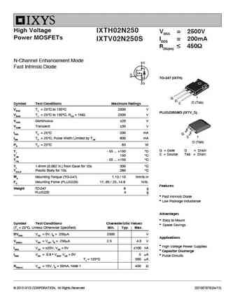
High Voltage IXTH02N250 VDSS = 2500V Power MOSFETs ID25 = 200mA IXTV02N250S RDS(on) 450 N-Channel Enhancement Mode Fast Intrinsic Diode TO-247 (IXTH) G D D (Tab) S Symbol Test Conditions Maximum Ratings VDSS TJ = 25 C to 150 C 2500 V PLUS220SMD (IXTV_S) VDGR TJ = 25 C to 150 C, RGS = 1M 2500 V VGSS Continuous 20 V VGSM Transient
0.20. Size:180K ixys
ixbh2n250.pdf

Advance Technical Information High Voltage, High Gain VCES = 2500V IXBH2N250 BIMOSFETTM IXBT2N250 IC110 = 2A VCE(sat) 3.50V Monolithic Bipolar MOS Transistor TO-247 (IXBH) Symbol Test Conditions Maximum Ratings VCES TC = 25 C to 150 C 2500 V VCGR TJ = 25 C to 150 C, RGE = 1M 2500 V G C (TAB) C VGES Continuous 20 V E VGEM Transient 30 V IC
0.21. Size:184K ixys
ixta02n250hv.pdf
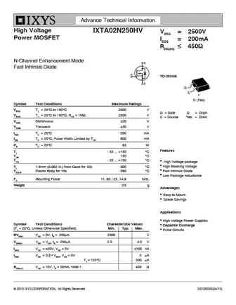
Advance Technical Information High Voltage IXTA02N250HV VDSS = 2500V Power MOSFET ID25 = 200mA RDS(on) 450 N-Channel Enhancement Mode Fast Intrinsic Diode TO-263AB G S D (Tab) Symbol Test Conditions Maximum Ratings VDSS TJ = 25 C to 150 C 2500 V G = Gate D = Drain VDGR TJ = 25 C to 150 C, RGS = 1M 2500 V S = Source Tab = Drain VGSS
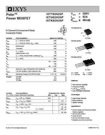
0.22. Size:294K ixys
ixtk82n25p ixtq82n25p ixtt82n25p.pdf
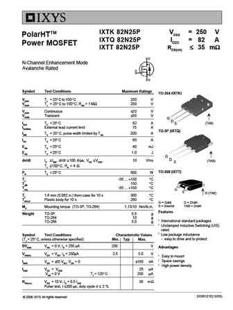
IXTK 82N25P VDSS = 250 V PolarHTTM IXTQ 82N25P ID25 = 82 A Power MOSFET IXTT 82N25P RDS(on) 35 m N-Channel Enhancement Mode Avalanche Rated Symbol Test Conditions Maximum Ratings TO-264 (IXTK) VDSS TJ = 25 C to 150 C 250 V VDGR TJ = 25 C to 150 C; RGS = 1 M 250 V VGSS Continuous 20 V VGSM Transient 30 V G D ID25 TC = 25
0.23. Size:252K ixys
ixta42n25p ixtp42n25p ixtq42n25p.pdf
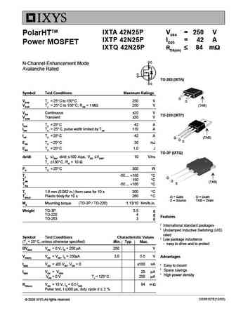
IXTA 42N25P VDSS = 250 V PolarHTTM IXTP 42N25P ID25 = 42 A Power MOSFET IXTQ 42N25P RDS(on) 84 m N-Channel Enhancement Mode Avalanche Rated TO-263 (IXTA) Symbol Test Conditions Maximum Ratings G VDSS TJ = 25 C to 150 C 250 V S VDGR TJ = 25 C to 150 C; RGS = 1 M 250 V (TAB) VGS Continuous 20 V TO-220 (IXTP) VGSM Transient 3
0.24. Size:189K utc
12n25.pdf

UNISONIC TECHNOLOGIES CO., LTD 12N25 Power MOSFET 12A, 250V N-CHANNEL POWER MOSFET DESCRIPTION The UTC 12N25 is an N-channel mode power MOSFET using UTC s advanced technology to provide customers with planar stripe and DMOS technology. This technology specializes in allowing a minimum on-state resistance and superior switching performance. It also can withstand high energy
0.25. Size:163K isahaya
rt2n25m.pdf
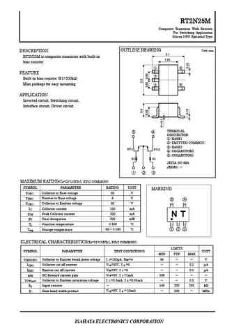
RT2N25M Composite Transistor With Resistor For Switching Application Silicon NPN Epitaxial Type OUTLINE DRAWING Unit mm DESCRIPTION 2.1 RT2N25M is composite transistor with built-in 1.25 bias resistor. FEATURE Built-in bias resistor (R1=200k ) Mini package for easy mounting APPLICATION Inverted circuit, Switching circuit, Interface circu
0.26. Size:143K samhop
sdu02n25 sdd02n25.pdf
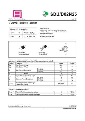
Green Product SDU/D02N25 a S mHop Microelectronics C orp. Ver 1.1 N-Channel Field Effect Transistor FEATURES PRODUCT SUMMARY Super high dense cell design for low RDS(ON). VDSS ID RDS(ON) ( ) Typ Rugged and reliable. 250V 2A 3.2 @ VGS=10V Suface Mount Package. G S SDU SERIES SDD SERIES TO - 252AA(D-PAK) TO - 251(I-PAK) ABSOLUTE MAXIMUM RATINGS (TA=25 C unless otherwise noted)
0.27. Size:151K semtech
2n25550 2n25551.pdf
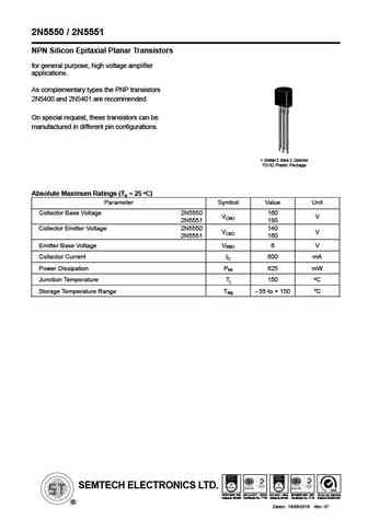
2N5550 / 2N5551 NPN Silicon Epitaxial Planar Transistors for general purpose, high voltage amplifier applications. As complementary types the PNP transistors 2N5400 and 2N5401 are recommended. On special request, these transistors can be manufactured in different pin configurations. 1. Emitter 2. Base 3. Collector TO-92 Plastic Package O Absolute Maximum Ratings (Ta = 25 C)
0.28. Size:1162K truesemi
tsa82n25m.pdf
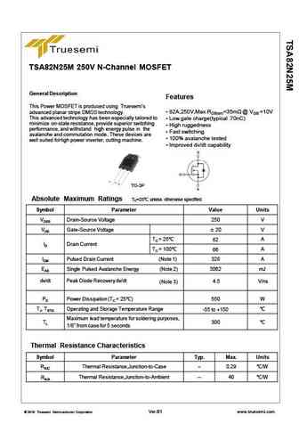
TSA82N25M 250V N-Channel MOSFET General Description Features This Power MOSFET is produced using Truesemi s 82A,250V,Max.RDS(on)=35m @ VGS =10V advanced planar stripe DMOS technology. This advanced technology has been especially tailored to Low gate charge(typical 70nC) minimize on-state resistance, provide superior switching High ruggedness performance, and withstand h
0.29. Size:942K truesemi
tsk82n25m.pdf
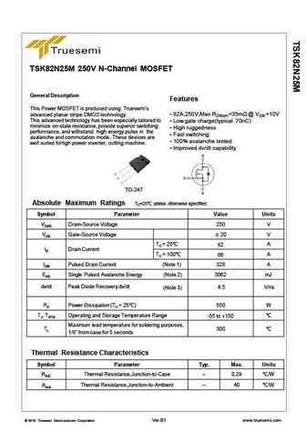
TSK82N25M 250V N-Channel MOSFET General Description Features This Power MOSFET is produced using Truesemi s 82A,250V,Max.RDS(on)=35m @ VGS =10V advanced planar stripe DMOS technology. This advanced technology has been especially tailored to Low gate charge(typical 70nC) minimize on-state resistance, provide superior switching High ruggedness performance, and withstand
0.30. Size:416K way-on
wm02n25m.pdf
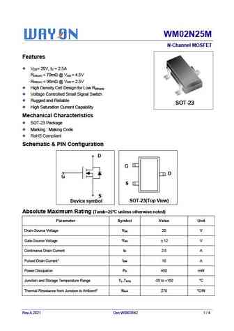
WM02N25M N-Channel MOSFET Features V = 20V, I = 2.5A DS D R
0.31. Size:819K cn hunteck
hga1k2n25ml.pdf
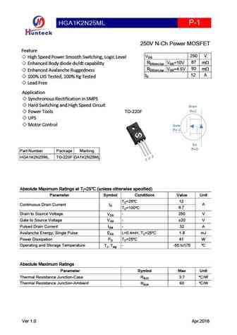
HGA1K2N25ML P-1 250V N-Ch Power MOSFET Feature 250 V VDS High Speed Power Smooth Switching, Logic Level 87 RDS(on),typ VGS=10V m Enhanced Body diode dv/dt capability 93 RDS(on),typ VGS=4.5V m Enhanced Avalanche Ruggedness 12 A ID 100% UIS Tested, 100% Rg Tested Lead Free Application Synchronous Rectification in SMPS Hard Switching and High Spe
0.32. Size:823K cn hunteck
hgp1k2n25ml.pdf
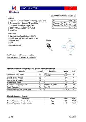
HGP1K2N25ML P-1 250V N-Ch Power MOSFET Feature 250 V VDS High Speed Power Smooth Switching, Logic Level 87 RDS(on),typ VGS=10V m Enhanced Body diode dv/dt capability 93 RDS(on),typ VGS=4.5V m Enhanced Avalanche Ruggedness 25 A ID 100% UIS Tested, 100% Rg Tested Lead Free Application Synchronous Rectification in SMPS Hard Switching and High Spe
0.33. Size:522K cn hmsemi
hm2n25.pdf

HM2N25 N-Channel Enhancement Mode Power MOSFET Description The HM2N25 uses advanced trench technology and design to provide excellent RDS(ON) with low gate charge. It can be used in a wide variety of applications. General Features VDS = 250V,ID =2A Schematic diagram RDS(ON)
Otros transistores... 2N249
, 2N2490
, 2N2491
, 2N2492
, 2N2493
, 2N2494
, 2N2495
, 2N2496
, MJE350
, 2N250
, 2N2501
, 2N2509
, 2N250A
, 2N251
, 2N2510
, 2N2511
, 2N2512
.