BUL52AFI Equivalente. Reemplazo. Hoja de especificaciones. Principales características
Número de Parte: BUL52AFI
Material: Si
Polaridad de transistor: NPN
ESPECIFICACIONES MÁXIMAS
Disipación total del dispositivo (Pc): 45 W
Tensión colector-base (Vcb): 1000 V
Tensión colector-emisor (Vce): 500 V
Corriente del colector DC máxima (Ic): 6 A
CARACTERÍSTICAS ELÉCTRICAS
Encapsulados: TO220F
Búsqueda de reemplazo de BUL52AFI
- Selecciónⓘ de transistores por parámetros
BUL52AFI datasheet
bul52asmd.pdf

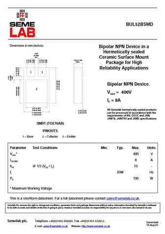
BUL52ASMD Dimensions in mm (inches). Bipolar NPN Device in a Hermetically sealed 0.89 (0.035) min. Ceramic Surface Mount 3.70 (0.146) 3.70 (0.146) 3.60 (0.142) 3.41 (0.134) 3.41 (0.134) Max. Package for High Reliability Applications 1 3 Bipolar NPN Device. 2 VCEO = 500V IC = 6A 9.67 (0.381) All Semelab hermetically sealed products 9.38 (0.369) 0.50 (0.020) 0.26 (
bul52a.pdf
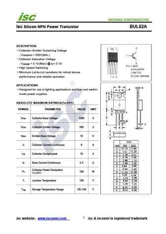
isc Silicon NPN Power Transistor BUL52A DESCRIPTION Collector Emitter Sustaining Voltage V = 500V(Min.) CEO(SUS) Collector Saturation Voltage V = 0.1V(Max) @ I = 0.1A CE(sat) C High Speed Switching Minimum Lot-to-Lot variations for robust device performance and reliable operation APPLICATIONS Designed for use in lighting applications and low cost switch- mode power
bul52bsmd.pdf
BUL52BSMD Dimensions in mm (inches). Bipolar NPN Device in a Hermetically sealed 0.89 (0.035) min. Ceramic Surface Mount 3.70 (0.146) 3.70 (0.146) 3.60 (0.142) 3.41 (0.134) 3.41 (0.134) Max. Package for High Reliability Applications 1 3 Bipolar NPN Device. 2 VCEO = 400V IC = 8A 9.67 (0.381) All Semelab hermetically sealed products 9.38 (0.369) 0.50 (0.020) 0.26 (
bul52b.pdf
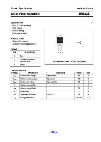
Product Specification www.jmnic.com Silicon Power Transistors BUL52B DESCRIPTION With TO-220C package High voltage Fast switching High energy rating APPLICATIONS Designed for use in electronic ballast applications PINNING PIN DESCRIPTION 1 Base Collector;connected to 2 mounting base 3 emitter LIMITING VALUES SYMBOL PARAMETER CONDITIONS VALUE UNIT V
Otros transistores... BUL49A, BUL49B, BUL50A, BUL50B, BUL510, BUL51A, BUL51B, BUL52A, BC639, BUL52B, BUL52BFI, BUL53A, BUL53B, BUL54A, BUL54AFI, BUL54B, BUL54BFI
History: BCX60-5 | CIL245
🌐 : EN ES РУ

Liste
Recientemente añadidas las descripciónes de los transistores:
BJT: GA1A4M | SBT42 | 2SA200-Y | 2SA200-O | 2SD882-Q | 2SD882-P | 2SD882-E | 2SC945-L | 2SC945-H | 2SC4226-R23 | 2SC3357-F | 2SC3357-E | 2SC3356-R26 | 2SC3356-R24 | 2SC3356-R23 | 2SB772-Q | 2SB772-P | 2SB772-E | 2SA1015-L | 2SA1015-H | HSS8550
Popular searches
irf620 | irfp350 | 13003 transistor | c458 transistor | 2sc1775 | 2n1305 | 2sc5242 | irf540 equivalent