F102 Equivalente. Reemplazo. Hoja de especificaciones. Principales características
Número de Parte: F102
Material: Si
Polaridad de transistor: NPN
ESPECIFICACIONES MÁXIMAS
Disipación total del dispositivo (Pc): 85 W
Tensión colector-base (Vcb): 60 V
Tensión colector-emisor (Vce): 60 V
Corriente del colector DC máxima (Ic): 4 A
Temperatura operativa máxima (Tj): 175 °C
CARACTERÍSTICAS ELÉCTRICAS
Transición de frecuencia (fT): 1 MHz
Ganancia de corriente contínua (hFE): 10
Encapsulados: TO53
Búsqueda de reemplazo de F102
- Selecciónⓘ de transistores por parámetros
F102 datasheet
..1. Size:455K fairchild semi
fcp25n60n f102.pdf 

March 2013 FCP25N60N_F102 N-Channel SupreMOS MOSFET 600 V, 25 A, 125 m Features Description RDS(on) = 107 m (Typ.)@ VGS = 10 V, ID = 12.5 A The SupreMOS MOSFET is Fairchild Semiconductor s next- generation of high voltage super-junction (SJ) technology Ultra Low Gate Charge (Typ. Qg = 57 nC) employing a deep trench filling process that differentiate it from
..2. Size:750K fairchild semi
fdp045n10a f102 fdi045n10a f102.pdf

July 2011 FDP045N10A_F102 / FDI045N10A_F102 N-Channel PowerTrench MOSFET 100V, 164A, 4.5m Features Description RDS(on) = 3.8m ( Typ.)@ VGS = 10V, ID = 100A This N-Channel MOSFET is produced using Fairchild Semiconductor s advance PowerTrench process that has been Fast Switching Speed especially tailored to minimize the on-state resistance and yet maintain superio
..3. Size:658K fairchild semi
fdp020n06b f102.pdf

January 2012 FDP020N06B_F102 N-Channel PowerTrench MOSFET 60V, 313A, 2m Features Description RDS(on) = 1.65m ( Typ.) at VGS = 10V, ID = 100A This N-Channel MOSFET is produced using Fairchild Semicon- ductor s advanced PowerTrench process that has been tailored Low FOM RDS(on) *QG to minimize the on-state resistance while maintaining superior switching performance
..4. Size:317K fairchild semi
fdp150n10a f102.pdf

July 2011 FDP150N10A_F102 tm N-Channel PowerTrench MOSFET 100V, 50A, 15m Features Description RDS(on) = 12.5m ( Typ.)@ VGS = 10V, ID = 50A This N-Channel MOSFET is produced using Fairchild Semiconductor s advance PowerTrench process that has been Fast Switching Speed especially tailored to minimize the on-state resistance and yet maintain superior switching performa
..5. Size:320K fairchild semi
fdp085n10a f102.pdf
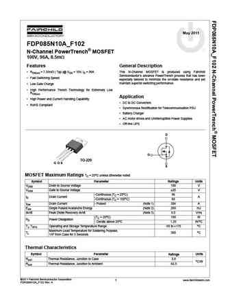
May 2011 FDP085N10A_F102 N-Channel PowerTrench MOSFET 100V, 96A, 8.5m Features General Description RDS(on) = 7.35m ( Typ.)@ VGS = 10V, ID = 96A This N-Channel MOSFET is produced using Fairchild Semiconductor s advance PowerTrench process that has been Fast Switching Speed especially tailored to minimize the on-state resistance and yet maintain superior switching perf
..6. Size:399K fairchild semi
fdp083n15a f102.pdf

March 2013 FDP083N15A _F102 N-Channel PowerTrench MOSFET 150 V, 117 A, 8.3 m Features Description RDS(on) = 6.85 m ( Typ.)@ VGS = 10 V, ID = 75 A This N-Channel MOSFET is produced using Fairchild Semiconductor s advanced PowerTrench process that has Fast Switching Speed been tailored to minimize the on-state resistance while maintain- ing superior switching perfo
..7. Size:312K fairchild semi
fdp075n15a f102 fdb075n15a.pdf

October 2012 FDP075N15A_F102 / FDB075N15A N-Channel PowerTrench MOSFET 150V, 130A, 7.5m Features Description RDS(on) = 6.25m ( Typ.)@ VGS = 10V, ID = 100A This N-Channel MOSFET is produced using Fairchild Semiconductor s advanced PowerTrench process that has Fast Switching been especially tailored to minimize the on-state resistance and yet maintain superior switc
..8. Size:421K fairchild semi
fci25n60n f102.pdf
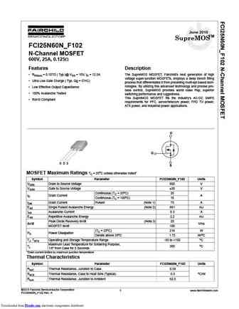
June 2010 TM SupreMOS FCI25N60N_F102 tm N-Channel MOSFET 600V, 25A, 0.125 Features Description RDS(on) = 0.107 ( Typ.)@ VGS = 10V, ID = 12.5A The SupreMOS MOSFET, Fairchild s next generation of high voltage super-junction MOSFETs, employs a deep trench filling Ultra Low Gate Charge ( Typ. Qg = 57nC) process that differentiates it from preceding multi-epi based tech-
..9. Size:641K fairchild semi
fdp030n06b f102.pdf

November 2013 FDP030N06B_F102 N-Channel PowerTrench MOSFET 60 V, 195 A, 3.1 m Features Description RDS(on) = 2.67 m (Typ.) @ VGS = 10 V, ID = 100 A This N-Channel MOSFET is produced using Fairchild Semicon- ductor s advanced PowerTrench process that has been tai- Low FOM RDS(on) * QG lored to minimize the on-state resistance while maintaining superior switching perfor
..10. Size:748K onsemi
fdp030n06b f102.pdf

Is Now Part of To learn more about ON Semiconductor, please visit our website at www.onsemi.com Please note As part of the Fairchild Semiconductor integration, some of the Fairchild orderable part numbers will need to change in order to meet ON Semiconductor s system requirements. Since the ON Semiconductor product management systems do not have the ability to manage part nomenclatur
0.1. Size:55K motorola
mrf1029r.pdf
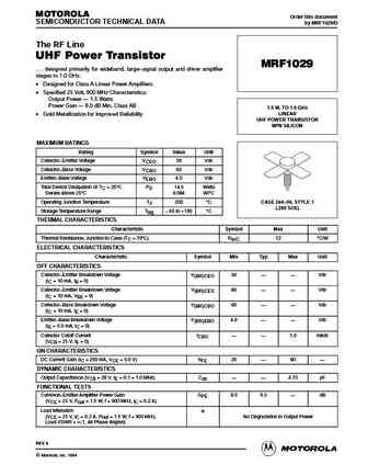
MOTOROLA Order this document SEMICONDUCTOR TECHNICAL DATA by MRF1029/D The RF Line UHF Power Transistor MRF1029 . . . designed primarily for wideband, large signal output and driver amplifier stages to 1.0 GHz. Designed for Class A Linear Power Amplifiers Specified 25 Volt, 900 MHz Characteristics Output Power 1.5 Watts Power Gain 8.0 dB Min, Class AB 1.5 W, TO 1
0.2. Size:55K motorola
mrf1029.pdf

MOTOROLA Order this document SEMICONDUCTOR TECHNICAL DATA by MRF1029/D The RF Line UHF Power Transistor MRF1029 . . . designed primarily for wideband, large signal output and driver amplifier stages to 1.0 GHz. Designed for Class A Linear Power Amplifiers Specified 25 Volt, 900 MHz Characteristics Output Power 1.5 Watts Power Gain 8.0 dB Min, Class AB 1.5 W, TO 1
0.3. Size:270K motorola
mpf102rev0d.pdf
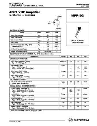
MOTOROLA Order this document SEMICONDUCTOR TECHNICAL DATA by MPF102/D JFET VHF Amplifier N Channel Depletion MPF102 1 DRAIN 3 GATE 2 SOURCE MAXIMUM RATINGS Rating Symbol Value Unit Drain Source Voltage VDS 25 Vdc 1 2 3 Drain Gate Voltage VDG 25 Vdc Gate Source Voltage VGS 25 Vdc CASE 29 04, STYLE 5 Gate Current IG 10 mAdc TO 92 (TO 226AA) Total Device D
0.4. Size:657K fairchild semi
fcp190n60 gf102.pdf

December 2013 FCP190N60_GF102 N-Channel SuperFET II MOSFET 600 V, 20.2 A, 199 m Features Description 650 V @ TJ = 150 C SuperFET II MOSFET is Fairchild Semiconductor s brand-new high voltage super-junction (SJ) MOSFET family that is utilizing Typ. RDS(on) = 170 m charge balance technology for outstanding low on-resistance Ultra Low Gate Charge (Typ. Qg = 57 nC)
0.5. Size:26K fairchild semi
mpf102.pdf

MPF102 N-Channel RF Amplifier This device is designed for electronic switching applications such as low ON resistance analog switching. Sourced from process 50. TO-92 1 1. Drain 2. Source 3. Gate Absolute Maximum Ratings * Ta=25 C unless otherwise noted Symbol Parameter Value Units VDG Drain-Gate Voltage 25 V VGS Gate-Source Voltage -25 V IGF Forward Gate Current 10 mA TJ
0.6. Size:621K onsemi
fcp190n60 gf102.pdf

Is Now Part of To learn more about ON Semiconductor, please visit our website at www.onsemi.com Please note As part of the Fairchild Semiconductor integration, some of the Fairchild orderable part numbers will need to change in order to meet ON Semiconductor s system requirements. Since the ON Semiconductor product management systems do not have the ability to manage part nomenclatur
0.7. Size:146K onsemi
mpf102.pdf
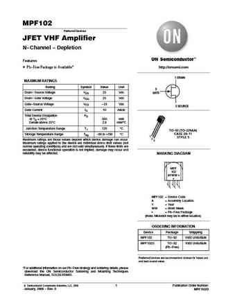
MPF102 Preferred Devices JFET VHF Amplifier N-Channel - Depletion Features Pb-Free Package is Available* http //onsemi.com 1 DRAIN MAXIMUM RATINGS Rating Symbol Value Unit 3 Drain-Source Voltage VDS 25 Vdc GATE Drain-Gate Voltage VDG 25 Vdc Gate-Source Voltage VGS -25 Vdc 2 SOURCE Gate Current IG 10 mAdc Total Device Dissipation PD @ TA = 25 C 350 mW Derate above 25 C 2
0.8. Size:458K silikron
ssf1020.pdf

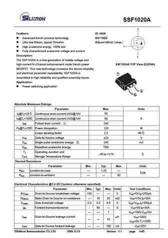
SSF1020 Feathers ID =60A Advanced trench process technology BV=100V Ultra low Rdson, typical 16mohm Rdson=16m Typ. High avalanche energy, 100% test Fully characterized avalanche voltage and current Description The SSF1020 is a new generation of middle voltage and high current N Channel enhancement mode trench power MOSFET. This new technology i
0.9. Size:685K silikron
ssf1020d.pdf

SSF1020D Main Product Characteristics VDSS 100V RDS(on) 16m (typ.) ID 60A DPAK Ma rk in g an d pi n Sc h ema t ic diag r am Assignment Features and Benefits Advanced trench MOSFET process technology Special designed for PWM, load switching and general purpose applications Ultra low on-resistance with low gate charge Fast switching and reverse body re
0.10. Size:453K silikron
ssf1020a.pdf
SSF1020A Feathers ID =60A Advanced trench process technology BV=100V Ultra low Rdson, typical 16mohm Rdson=20m max. High avalanche energy, 100% test Fully characterized avalanche voltage and current Description The SSF1020A is a new generation of middle voltage and high current N Channel enhancement mode trench power SSF1020A TOP View (D2PAK) MOSFET. This ne
Otros transistores... EW58-2
, EW59
, EW69
, EW721
, EW722
, EW723
, EWQ282
, F101
, A1013
, F103
, F104
, F105
, F106
, F107
, F108
, F109
, F110
.
History: ZXTN2020F
| DK53AD
| HM117
| 2SA1774EB
