J461 Datasheet. Equivalente. Reemplazo. Hoja de especificaciones. Principales características
Número de Parte: J461 📄📄
Material: Si
Polaridad de transistor: NPN
ESPECIFICACIONES MÁXIMAS
Disipación total del dispositivo (Pc): 0.15 W
Tensión colector-base (Vcb): 30 V
Tensión emisor-base (Veb): 2 V
Corriente del colector DC máxima (Ic): 0.025 A
Temperatura operativa máxima (Tj): 200 °C
CARACTERÍSTICAS ELÉCTRICAS
Ganancia de corriente contínua (hFE): 7
Encapsulados: TO22
📄📄 Copiar
Búsqueda de reemplazo de J461
- Selecciónⓘ de transistores por parámetros
J461 datasheet
2sj461a.pdf

DATA SHEET MOS FIELD EFFECT TRANSISTOR 2SJ461A P-CHANNEL MOSFET FOR HIGH SPEED SWITCHING DESCRIPTION The 2SJ461A is a switching device which can be driven directly by a 2.5 V power source. The 2SJ461A has excellent switching characteristics and is suitable for use as a high-speed switching device in digital circuit. FEATURES PACKAGE DRAWING (Unit mm) Can be driven by a
2sj461.pdf
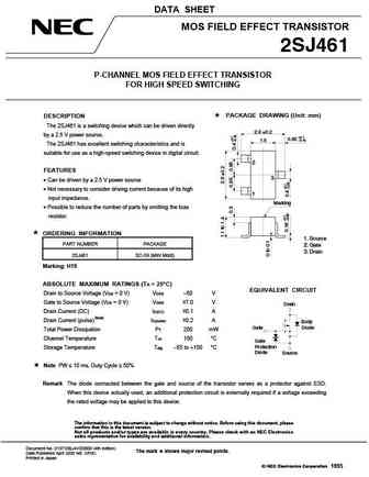
DATA SHEET MOS FIELD EFFECT TRANSISTOR 2SJ461 P-CHANNEL MOS FIELD EFFECT TRANSISTOR FOR HIGH SPEED SWITCHING PACKAGE DRAWING (Unit mm) DESCRIPTION The 2SJ461 is a switching device which can be driven directly 2.8 0.2 by a 2.5 V power source. +0.1 0.65 0.15 1.5 The 2SJ461 has excellent switching characteristics and is suitable for use as a high-speed switching device
sqj461ep.pdf
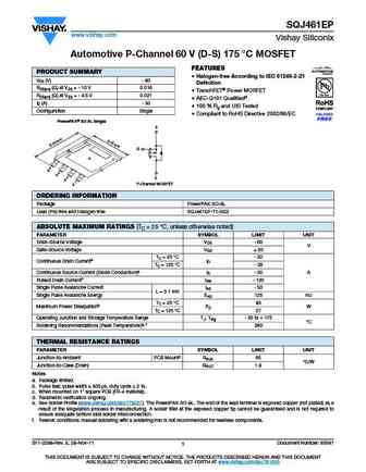
SQJ461EP www.vishay.com Vishay Siliconix Automotive P-Channel 60 V (D-S) 175 C MOSFET FEATURES PRODUCT SUMMARY Halogen-free According to IEC 61249-2-21 VDS (V) - 60 Definition RDS(on) ( ) at VGS = - 10 V 0.016 TrenchFET Power MOSFET RDS(on) ( ) at VGS = - 4.5 V 0.021 AEC-Q101 Qualifiedd ID (A) - 30 100 % Rg and UIS Tested Configuration Single Compliant
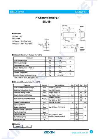
2sj461-3.pdf
SMD Type MOSFET P-Channel MOSFET 2SJ461 SOT-23-3 Unit mm +0.2 2.9 -0.1 +0.1 0.4-0.1 3 Features VDS (V) =-50V 1 2 ID =-0.1 A +0.02 +0.1 0.15 -0.02 0.95 -0.1 +0.1 RDS(ON) 50 (VGS =-4V) 1.9 -0.2 RDS(ON) 100 (VGS =-2.5V) 1. Gate 2. Source 3. Drain Absolute Maximum Ratings Ta = 25 Parameter Symbol Rating Unit Drain-Source Voltag
Otros transistores... IT2605, IT2904, IT2905, IT2906, IT2907, IT918, J24562, J460, 2N5551, J462, J463, J464, J465, J466, J581, J582, J583
History: IMD6AFRA | IMH20TR1G
🌐 : EN ES РУ

Liste
Recientemente añadidas las descripciónes de los transistores:
BJT: GA1A4M | SBT42 | 2SA200-Y | 2SA200-O | 2SD882-Q | 2SD882-P | 2SD882-E | 2SC945-L | 2SC945-H | 2SC4226-R23 | 2SC3357-F | 2SC3357-E | 2SC3356-R26 | 2SC3356-R24 | 2SC3356-R23 | 2SB772-Q | 2SB772-P | 2SB772-E | 2SA1015-L | 2SA1015-H | HSS8550
Popular searches
2sa747 | a1941 | 2sd424 datasheet | 2sc536 datasheet | bd140 transistor equivalent | tip122 transistor equivalent | irfz44n equivalent | 2n2923