2N43 Equivalente. Reemplazo. Hoja de especificaciones. Principales características
Número de Parte: 2N43
Material: Ge
Polaridad de transistor: PNP
ESPECIFICACIONES MÁXIMAS
Disipación total del dispositivo (Pc): 0.15 W
Tensión colector-base (Vcb): 45 V
Tensión emisor-base (Veb): 5 V
Corriente del colector DC máxima (Ic): 0.3 A
Temperatura operativa máxima (Tj): 85 °C
CARACTERÍSTICAS ELÉCTRICAS
Transición de frecuencia (fT): 1.3 MHz
Capacitancia de salida (Cc): 80 pF
Ganancia de corriente contínua (hFE): 53
Encapsulados: U10
Búsqueda de reemplazo de 2N43
- Selecciónⓘ de transistores por parámetros
2N43 datasheet
0.6. Size:59K vishay
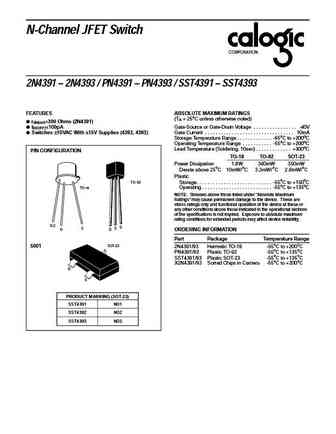
2n4391 pn4391 sst4391 2n4392 pn4392 sst4392 2n4393 pn4393 sst4393.pdf 
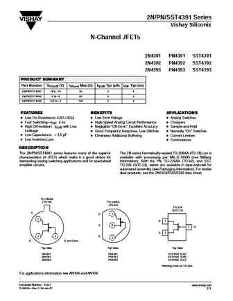
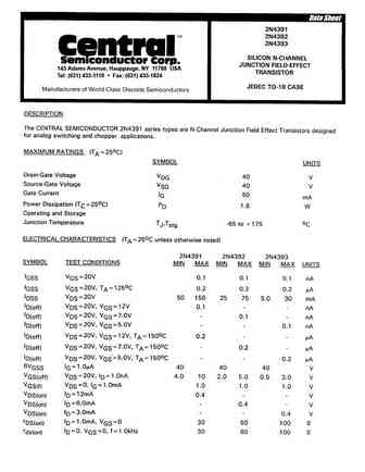
2N/PN/SST4391 Series Vishay Siliconix N-Channel JFETs 2N4391 PN4391 SST4391 2N4392 PN4392 SST4392 2N4393 PN4393 SST4393 PRODUCT SUMMARY Part Number VGS(off) (V) rDS(on) Max (W) ID(off) Typ (pA) tON Typ (ns) 2N/PN/SST4391 4 to 10 30 5 4 2N/PN/SST4392 2 to 5 60 5 4 2N/PN/SST4393 0.5 to 3 100 5 4 FEATURES BENEFITS APPLICATIONS D Low On-Resistance 4391
0.7. Size:75K vishay
2n4338 2n4339 2n4340 2n4341.pdf
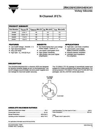
2N4338/4339/4340/4341 Vishay Siliconix N-Channel JFETs PRODUCT SUMMARY Part Number VGS(off) (V) V(BR)GSS Min (V) gfs Min (mS) IDSS Max (mA) 2N4338 -0.3 to -1 -50 0.6 0.6 2N4339 -0.6 to -1.8 -50 0.8 1.5 2N4340 -1 to -3 -50 1.3 3.6 2N4341 -2 to -6 -50 2 9 FEATURES BENEFITS APPLICATIONS D Low Cutoff Voltage 2N4338
0.8. Size:106K central
2n4391 2n4392 2n4393.pdf
145 Adams Avenue, Hauppauge, NY 11788 USA Tel (631) 435-1110 Fax (631) 435-1824 TM Central Semiconductor Corp. 145 Adams Avenue Hauppauge, NY 11788 USA Tel (631) 435-1110 Fax (631) 435-1824 www.centralsemi.com
0.9. Size:197K comset
2n3442-2n4347.pdf
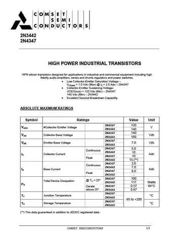
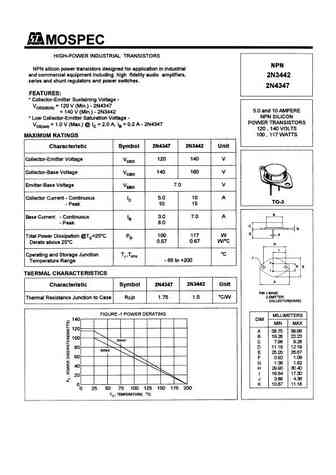
2N3442 2N4347 HIGH POWER INDUSTRIAL TRANSISTORS HIGH POWER INDUSTRIAL TRANSISTORS NPN silicon transistors designed for applications in industrial and commercial equipment including high fidelity audio amplifiers, series and shunts regulators and power switches. Low Collector-Emitter Saturation Voltage VCE(sat) = 1.0 Vdc (Max) @ IC = 2.0 Adc 2N4347 Collector-Emitter Susta
0.13. Size:49K semelab
2n4393dcsm.pdf
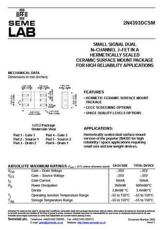
2N4393DCSM SEME LAB SMALL SIGNAL DUAL N CHANNEL J FET IN A HERMETICALLY SEALED CERAMIC SURFACE MOUNT PACKAGE FOR HIGH RELIABILITY APPLICATIONS MECHANICAL DATA Dimensions in mm (inches) 1.40 0.15 2.29 0.20 1.65 0.13 (0.055 0.006) (0.09 0.008) (0.065 0.005) FEATURES 2 3 HERMETIC CERAMIC SURFACE MOUNT 1 4 A PACKAGE 0.23 6 5 rad. (0.009) CECC SC
0.14. Size:15K semelab
2n4392.pdf
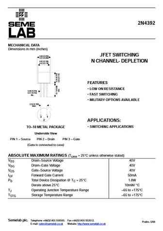
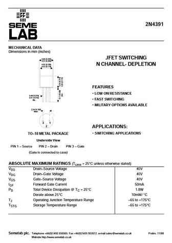
2N4392 MECHANICAL DATA Dimensions in mm (inches) JFET SWITCHING 5.84 (0.230) 5.31 (0.209) 4.95 (0.195) N CHANNEL- DEPLETION 4.52 (0.178) FEATURES LOW ON RESISTANCE 0.48 (0.019) 0.41 (0.016) FAST SWITCHING dia. MILITARY OPTIONS AVAILABLE 2.54 (0.100) Nom. 3 1 2 APPLICATIONS SWITCHING APPLICATIONS TO 18 METAL PACKAGE Underside View PIN 1 Source PIN 2
0.15. Size:13K semelab
2n4391.pdf
2N4391 MECHANICAL DATA Dimensions in mm (inches) JFET SWITCHING 5.84 (0.230) 5.31 (0.209) 4.95 (0.195) N CHANNEL- DEPLETION 4.52 (0.178) FEATURES LOW ON RESISTANCE 0.48 (0.019) 0.41 (0.016) FAST SWITCHING dia. MILITARY OPTIONS AVAILABLE 2.54 (0.100) Nom. 3 1 2 APPLICATIONS SWITCHING APPLICATIONS TO 18 METAL PACKAGE Underside View PIN 1 Source PIN 2
0.16. Size:229K semelab
2n4393c1a 2n4393c1b 2n4393c1c 2n4393c1d.pdf
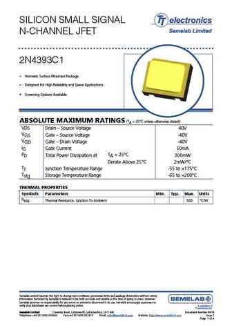
SILICON SMALL SIGNAL N-CHANNEL JFET 2N4393C1 Hermetic Surface Mounted Package. Designed For High Reliability and Space Applications. Screening Options Available. ABSOLUTE MAXIMUM RATINGS (TA = 25 C unless otherwise stated) VDS Drain Source Voltage 40V VGS Gate Source Voltage -40V VGD Gate Drain Voltage -40V IG Gate Current 50mA PD TA = 25 C
0.17. Size:18K calogic
2n4352.pdf
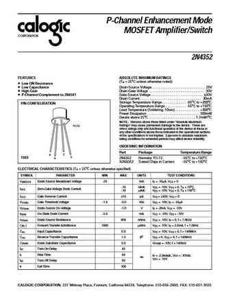
P-Channel Enhancement Mode MOSFET Amplifier/Switch CORPORATION 2N4352 FEATURES ABSOLUTE MAXIMUM RATINGS (T = 25oC unless otherwise noted) A Low ON Resistance Low Capacitance Drain-Source Voltage. . . . . . . . . . . . . . . . . . . . . . . . . . . . . 25V High Gain Drain-Gate Voltage . . . . . . . . . . . . . . . . . . . . . . . . . . . . . . 30V P-Chann
0.19. Size:19K calogic
2n4338 2n4339 2n4340 2n4341.pdf
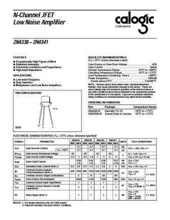
N-Channel JFET Low Noise Amplifier CORPORATION 2N4338 2N4341 FEATURES ABSOLUTE MAXIMUM RATINGS (T = 25oC unless otherwise noted) A Exceptionally High Figure of Merit Radiation Immunity Gate-Source or Gate-Drain Voltage . . . . . . . . . . . . . . . . -50V Extremely Low Noise and Capacitance Gate Current . . . . . . . . . . . . . . . . . . . . . . . . . . . . .
0.20. Size:217K linear-systems
2n4351.pdf
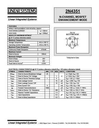
2N4351 N-CHANNEL MOSFET Linear Integrated Systems ENHANCEMENT MODE FEATURES DIRECT REPLACEMENT FOR INTERSIL 2N4351 HIGH DRAIN CURRENT ID = 100mA TO-72 HIGH GAIN gfs = 1000 S BOTTOM VIEW ABSOLUTE MAXIMUM RATINGS1 @ 25 C (unless otherwise stated) G 2 3 D Maximum Temperatures Storage Temperature -65 to +200 C Operating Junction Temperature -55 to +150 C 1 4 S
0.21. Size:183K inchange semiconductor
2n4347.pdf
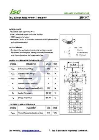
isc Silicon NPN Power Transistor 2N4347 DESCRIPTION Excellent Safe Operating Area Low Collector-Emitter Saturation Voltage 100% avalanche tested Minimum Lot-to-Lot variations for robust device performance and reliable operation. APPLICATIONS Designed for application in industrial and commercial equipment including high fidelity audio amplifier,series and shunt regulators and
0.22. Size:183K inchange semiconductor
2n4348.pdf
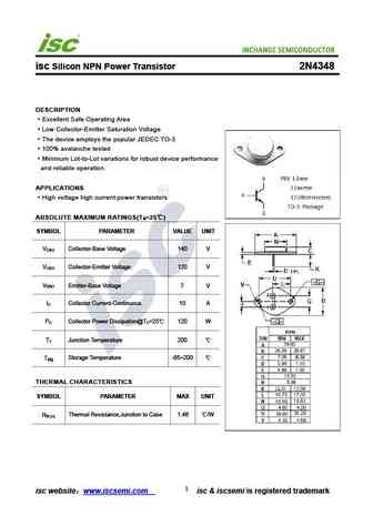
isc Silicon NPN Power Transistor 2N4348 DESCRIPTION Excellent Safe Operating Area Low Collector-Emitter Saturation Voltage The device employs the popular JEDEC TO-3 100% avalanche tested Minimum Lot-to-Lot variations for robust device performance and reliable operation. APPLICATIONS High voltage high current power transistors ABSOLUTE MAXIMUM RATINGS(T =25 ) a SYMBOL P
0.23. Size:38K inchange semiconductor
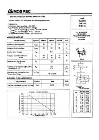
2n4399.pdf

INCHANGE Semiconductor isc Product Specification isc Silicon PNP Power Transistors 2N4399 DESCRIPTION Low Collector Saturation Voltage- VCE(sat)= -1.0V(Max.)@ IC= -15A Wide Area of Safe Operation Complement to Type 2N5302 APPLICATIONS Designed for use in power amplifier and switching circuits. ABSOLUTE MAXIMUM RATINGS(Ta=25 ) SYMBOL PARAMETER VALUE UNIT V Coll
0.24. Size:181K inchange semiconductor
2n4395.pdf
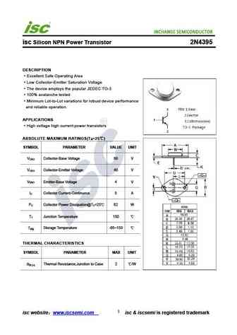
isc Silicon NPN Power Transistor 2N4395 DESCRIPTION Excellent Safe Operating Area Low Collector-Emitter Saturation Voltage The device employs the popular JEDEC TO-3 100% avalanche tested Minimum Lot-to-Lot variations for robust device performance and reliable operation. APPLICATIONS High voltage high current power transistors ABSOLUTE MAXIMUM RATINGS(T =25 ) a SYMBOL P
0.25. Size:185K inchange semiconductor
2n4387.pdf
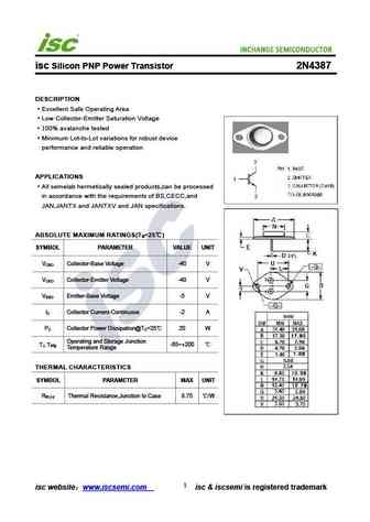
isc Silicon PNP Power Transistor 2N4387 DESCRIPTION Excellent Safe Operating Area Low Collector-Emitter Saturation Voltage 100% avalanche tested Minimum Lot-to-Lot variations for robust device performance and reliable operation APPLICATIONS All semelab hermetically sealed products,can be processed in accordance with the requirements of BS,CECC,and JAN,JANTX and JANTXV and JA
0.26. Size:38K inchange semiconductor
2n4398.pdf
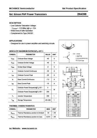
INCHANGE Semiconductor isc Product Specification isc Silicon PNP Power Transistors 2N4398 DESCRIPTION Low Collector Saturation Voltage- VCE(sat)= -1.0V(Max.)@ IC= -15A Wide Area of Safe Operation Complement to Type 2N5301 APPLICATIONS Designed for use in power amplifier and switching circuits. ABSOLUTE MAXIMUM RATINGS(Ta=25 ) SYMBOL PARAMETER VALUE UNIT V Coll
0.27. Size:182K inchange semiconductor
2n4396.pdf
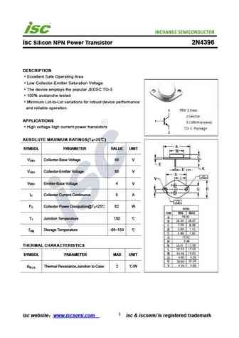
isc Silicon NPN Power Transistor 2N4396 DESCRIPTION Excellent Safe Operating Area Low Collector-Emitter Saturation Voltage The device employs the popular JEDEC TO-3 100% avalanche tested Minimum Lot-to-Lot variations for robust device performance and reliable operation. APPLICATIONS High voltage high current power transistors ABSOLUTE MAXIMUM RATINGS(T =25 ) a SYMBOL P
0.28. Size:185K inchange semiconductor
2n4388.pdf

isc Silicon PNP Power Transistor 2N4388 DESCRIPTION Excellent Safe Operating Area Low Collector-Emitter Saturation Voltage 100% avalanche tested Minimum Lot-to-Lot variations for robust device performance and reliable operation APPLICATIONS All semelab hermetically sealed products,can be processed in accordance with the requirements of BS,CECC,and JAN,JANTX and JANTXV and JA
0.29. Size:121K inchange semiconductor
2n4398 2n4399 2n5745.pdf
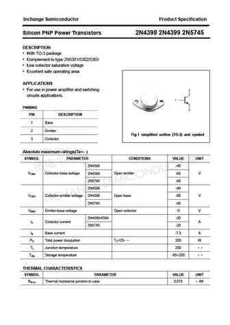
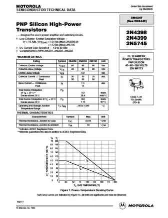
Inchange Semiconductor Product Specification Silicon PNP Power Transistors 2N4398 2N4399 2N5745 DESCRIPTION With TO-3 package Complement to type 2N5301/5302/5303 Low collector saturation voltage Excellent safe operating area APPLICATIONS For use in power amplifier and switching circuits applications. PINNING PIN DESCRIPTION 1 Base 2 Emitter Fig.1 simplified o
Otros transistores... 2N4292
, 2N4293
, 2N4294
, 2N4295
, 2N4296
, 2N4297
, 2N4298
, 2N4299
, BC549
, 2N4300
, 2N4301
, 2N4305
, 2N4306
, 2N4307
, 2N4308
, 2N4309
, 2N431
.
History: 2N4301
| HSE185
| KT209I