MN26 Equivalente. Reemplazo. Hoja de especificaciones. Principales características
Número de Parte: MN26
Material: Ge
Polaridad de transistor: PNP
ESPECIFICACIONES MÁXIMAS
Disipación total del dispositivo (Pc): 45 W
Tensión colector-base (Vcb): 40 V
Corriente del colector DC máxima (Ic): 3 A
Temperatura operativa máxima (Tj): 85 °C
CARACTERÍSTICAS ELÉCTRICAS
Transición de frecuencia (fT): 0.1 MHz
Ganancia de corriente contínua (hFE): 35
Encapsulados: TO3
Búsqueda de reemplazo de MN26
- Selecciónⓘ de transistores por parámetros
MN26 datasheet
0.1. Size:325K diodes
dmn26d0udj.pdf 
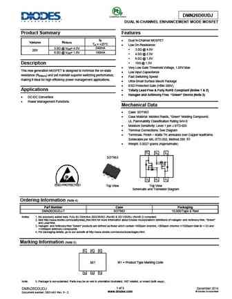
DMN26D0UDJ DUAL N-CHANNEL ENHANCEMENT MODE MOSFET Product Summary Features ID Dual N-Channel MOSFET V(BR)DSS RDS(on) TA = +25 C Low On-Resistance 3.0 @ VGS= 4.5V 240mA 3.0 @ 4.5V 20V 180mA 6.0 @ VGS= 1.8V 4.0 @ 2.5V 6.0 @ 1.8V 10 @ 1.5V Description Very Low Gate Threshold Voltage, 1.05V Max This new
0.2. Size:139K diodes
dmn2600ufb.pdf
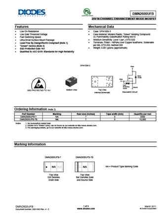
DMN2600UFB 25V N-CHANNEL ENHANCEMENT MODE MOSFET Features Mechanical Data Low On-Resistance Case DFN1006-3 Low Gate Threshold Voltage Case Material Molded Plastic, Green Molding Compound. UL Flammability Classification Rating 94V-0 Fast Switching Speed Moisture Sensitivity Level 1 per J-STD-020 Ultra-Small Surface Mount Package Terminals
0.3. Size:145K diodes
dmn26d0ut.pdf
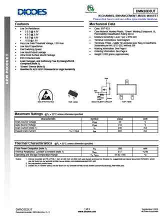
DMN26D0UT N-CHANNEL ENHANCEMENT MODE MOSFET Please click here to visit our online spice models database. Features Mechanical Data Low On-Resistance Case SOT-523 3.0 @ 4.5V Case Material Molded Plastic, Green Molding Compound. UL Flammability Classification Rating 94V-0 4.0 @ 2.5V Moisture Sensitivity Level 1 per J-STD-020 6.0 @ 1.8V
0.4. Size:122K diodes
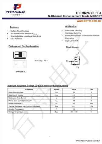
dmn26d0ufb4.pdf
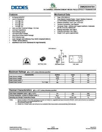
DMN26D0UFB4 N-CHANNEL ENHANCEMENT MODE FIELD EFFECT TRANSISTOR Features Mechanical Data N-Channel MOSFET Case DFN1006H4-3 Low On-Resistance Case Material Molded Plastic, Green Molding Compound. UL Flammability Classification Rating 94V-0 3.0 @ 4.5V Moisture Sensitivity Level 1 per J-STD-020 4.0 @ 2.5V Terminal Connections See Diag
0.5. Size:685K way-on
wml26n65c4 wmo26n65c4 wmk26n65c4 wmn26n65c4 wmm26n65c4 wmj26n65c4.pdf

WML26N65C4, WMO26N6 WM C4 W 65C4, MK26N65C WMN2 MJ26N65C 26N65C4, WMM26N65C4, WM C4 650V 0.16 S T V Super Junction Power MOSFET Descrip ption WMOSTM C4 is Wa 4th generation super ayon s n junction MOSFET fa that is utilizing charge M amily S balance te or extremely esistance echnology fo y low on-re S D D G G G S D G and low ga charge performanc WMOSTM
0.6. Size:681K way-on
wml26n60c4 wmk26n60c4 wmn26n60c4 wmm26n60c4 wmo26n60c4 wmj26n60c4.pdf

WML26N60C4, WMO26N6 WM C4 W 60C4, MK26N60C WMN2 MJ26N60C 26N60C4, WMM26N60C4, WM C4 600V 0.16 S T V Super Junction Power MOSFET Descrip ption WMOSTM C4 is Wa 4th generation super ayon s n junction MOSFET fa that is utilizing charge M amily S balance te or extremely esistance echnology fo y low on-re S D D G G G S D G and low ga charge performanc WMOSTM
0.7. Size:682K way-on
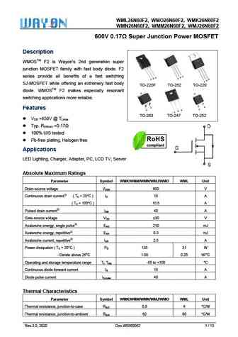
wml26n65f2 wmo26n65f2 wmk26n65f2 wmn26n65f2 wmm26n65f2 wmj26n65f2.pdf

WML2 N65F2, WM F2 26N65F2, WMO26N MK26N65F WMN2 N65F2, WM F2 26N65F2, WMM26N MJ26N65F 650V 0.17 S T V Super Junction Power MOSFET Descrip ption WMOSTM F2 is Wa 2nd generation super ayon s junction MOSFET fam with fa body di F2 M mily ast iode. S series pro all benefits of a fast switching ovide b f s S D D G G G S D G SJ-MOSFE while of an extremely fa
0.8. Size:659K way-on
wml26n65sr wmk26n65sr wmn26n65sr wmm26n65sr wmj26n65sr.pdf
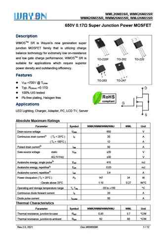
WML26N6 MK26N65S 65SR, WM SR WMN2 MJ26N65S 26N65SR, WMM26N65SR, WM SR 650V 0.17 S unction Power M T Super Ju MOSFET Descrip ption WMOSTM SR is Wa new generation super ayon s w junction MOSFET fa that is utilizing charge M amily S balance te or extremely esistance echnology fo y low on-re S D D G G G S D G T and low ga charge performanc WMOSTM SR is
0.9. Size:681K way-on
wml26n60c4 wmo26n60c4 wmk26n60c4 wmn26n60c4 wmm26n60c4 wmj26n60c4.pdf

WML26N60C4, WMO26N6 WM C4 W 60C4, MK26N60C WMN2 MJ26N60C 26N60C4, WMM26N60C4, WM C4 600V 0.16 S T V Super Junction Power MOSFET Descrip ption WMOSTM C4 is Wa 4th generation super ayon s n junction MOSFET fa that is utilizing charge M amily S balance te or extremely esistance echnology fo y low on-re S D D G G G S D G and low ga charge performanc WMOSTM
0.10. Size:679K way-on
wml26n60f2 wmo26n60f2 wmk26n60f2 wmn26n60f2 wmm26n60f2 wmj26n60f2.pdf
WML2 N60F2, WM F2 26N60F2, WMO26N MK26N60F WMN2 N60F2, WM F2 26N60F2, WMM26N MJ26N60F 600V 0.17 S T V Super Junction Power MOSFET Descrip ption WMOSTM F2 is Wa 2nd generation super ayon s junction MOSFET fam with fa body di F2 M mily ast iode. S series pro all benefits of a fast switching ovide b f s S D D G G G S D G SJ-MOSFE while of an extremely fa
0.11. Size:685K way-on
wml26n65c4 wmk26n65c4 wmn26n65c4 wmm26n65c4 wmo26n65c4 wmj26n65c4.pdf

WML26N65C4, WMO26N6 WM C4 W 65C4, MK26N65C WMN2 MJ26N65C 26N65C4, WMM26N65C4, WM C4 650V 0.16 S T V Super Junction Power MOSFET Descrip ption WMOSTM C4 is Wa 4th generation super ayon s n junction MOSFET fa that is utilizing charge M amily S balance te or extremely esistance echnology fo y low on-re S D D G G G S D G and low ga charge performanc WMOSTM
Otros transistores... MMUN2134LT2, MN13A, MN13B, MN13C, MN19, MN21, MN24, MN25, MJE340, MN28, MN29, MN32, MN48, MN49, MO810, MO816, MO818