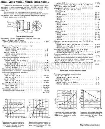
MP10 Equivalente. Reemplazo. Hoja de especificaciones. Principales características
Número de Parte: MP10
Material: Ge
Polaridad de transistor: NPN
ESPECIFICACIONES MÁXIMAS
Disipación total del dispositivo (Pc): 0.15 W
Tensión colector-base (Vcb): 15 V
Tensión colector-emisor (Vce): 15 V
Tensión emisor-base (Veb): 15 V
Corriente del colector DC máxima (Ic): 0.02 A
Temperatura operativa máxima (Tj): 85 °C
CARACTERÍSTICAS ELÉCTRICAS
Transición de frecuencia (fT): 1 MHz
Capacitancia de salida (Cc): 60 pF
Ganancia de corriente contínua (hFE): 15
Búsqueda de reemplazo de MP10
- Selecciónⓘ de transistores por parámetros
MP10 datasheet
cmp100n04 cmb100n04 cmi100n04.pdf
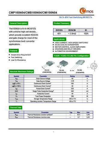
CMP100N04/CMB100N04/CMI100N04 N-Ch 40V Fast Switching MOSFETs General Description Product Summery The100N04 is N-ch MOSFE Ts BVDSS RDSON ID with extreme high cell density , 40V
dmp10h400sk3.pdf
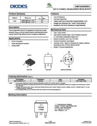
DMP10H400SK3 100V P-CHANNEL ENHANCEMENT MODE MOSFET Product Summary Features ID Low On-Resistance V(BR)DSS RDS(on) max TC = +25 C Low Input Capacitance 240m @ VGS = -10V -9A -100V Totally Lead-Free & Fully RoHS Compliant (Notes 1 & 2) -8A 300m @ VGS = -4.5V Halogen and Antimony Free. Green Device (Note 3) Qualified to AEC-Q101 Standards
zxmp10a18k.pdf
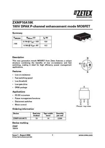
ZXMP10A18K 100V DPAK P-channel enhancement mode MOSFET Summary V(BR)DSS RDS(on) ( )ID (A) 0.150 @ VGS= -10V -5.9 -100 0.190 @ VGS= -6V -5.2 Description D This new generation trench MOSFET from Zetex features a unique structure combining the benefits of low on-resistance and fast G switching, making it ideal for high efficiency power management applications. Features S Low on
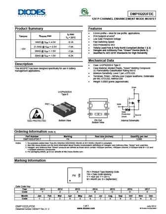
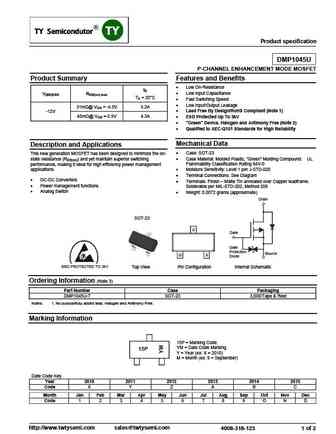
dmp1055ufdb.pdf
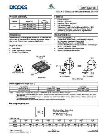
DMP1055UFDB DUAL P-CHANNEL ENHANCEMENT MODE MOSFET Product Summary Features Low On-Resistance ID MAX V(BR)DSS RDS(ON) max Low Input Capacitance TA = +25 C Low Profile, 0.6mm Max Height 59m @ VGS = -4.5V -3.9A ESD protected gate. -12V 81m @ VGS = -2.5V -3.3A Totally Lead-Free & Fully RoHS Compliant (Notes 1 & 2) 115m @ VGS = -1.8V -2.8A
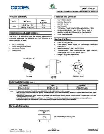
zxmp10a13fta.pdf
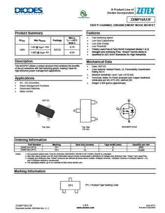
A Product Line of Diodes Incorporated ZXMP10A13F 100V P-CHANNEL ENHANCEMENT MODE MOSFET Product Summary Features Fast Switching Speed Max ID BVDSS Max RDS(ON) Package TA = +25 C Low Input Capacitance Note 5 Low Gate Charge Low Threshold 1.0 @ VGS= -10V -0.7A Totally Lead-Free & Fully RoHS Compliant (Notes 1 & 2) -100V SOT23 Halogen and Antim
dmp1005ufdf.pdf
DMP1005UFDF P-CHANNEL ENHANCEMENT MODE MOSFET Product Summary Features and Benefits 0.6mm Profile Ideal for Low Profile Applications ID Max BVDSS RDS(ON) Max PCB Footprint of 4mm2 TC = +25 C 8.5m @ VGS = -4.5V -26A Low Gate Threshold Voltage -12V -22A 12m @ VGS = -2.5V Low On-Resistance ESD Protected up to 8kV Totally Lead-Free &
dmp10h4d2s.pdf
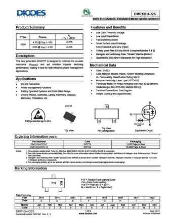
DMP10H4D2S 100V P-CHANNEL ENHANCEMENT MODE MOSFET Product Summary Features and Benefits Low Gate Threshold Voltage ID Low Input Capacitance BVDSS RDS(ON) TA = +25 C Fast Switching Speed 4.2 @ VGS = -10V -0.27A Small Surface Mount Package -100V 5.0 @ VGS = -4.0V -0.24A ESD Protected up to 2KV (HBM) Totally Lead-Free & Fully RoHS Compliant
dmp1045ufy4.pdf
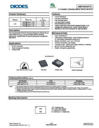
DMP1045UFY4 P-CHANNEL ENHANCEMENT MODE MOSFET Product Summary Features Low On-Resistance ID Low Input Capacitance V(BR)DSS RDS(on) max TA = 25 C Fast Switching Speed 32m @ VGS = -4.5V -5.5A Low Input/Output Leakage -12V 45m @ VGS = -2.5V -4.5A ESD Protected Up To 3kV Totally Lead-Free & Fully RoHS Compliant (Notes 1 & 2) 75m @ VGS = -1.8V -3.2A
zxmp10a18g.pdf
ZXMP10A18G 100V P-CHANNEL ENHANCEMENT MODE MOSFET SUMMARY V(BR)DSS = - 100V RDS(on) = 0.150 ; ID = - 3.7A DESCRIPTION This new generation of Trench MOSFETs from Zetex utilizes a unique structure that combines the benefits of low on-resistance with fast switching speed. This makes them ideal for high efficiency, low voltage, power management applications. FEATURES SOT223 Low on-r
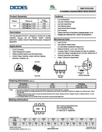
dmp1022ufdf.pdf
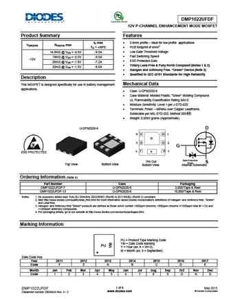
DMP1022UFDF 12V P-CHANNEL ENHANCEMENT MODE MOSFET Product Summary Features ID max 0.6mm profile ideal for low profile applications V(BR)DSS RDS(ON) max TA = +25 C PCB footprint of 4mm2 Low Gate Threshold Voltage 14.8m @ VGS = -4.5V -9.5A Fast Switching Speed 19m @ VGS = -2.5V -8.5A -12V ESD Protected Gate 26m @ VGS = -1.8V -7.2A To
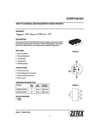
zxmp10a16k.pdf
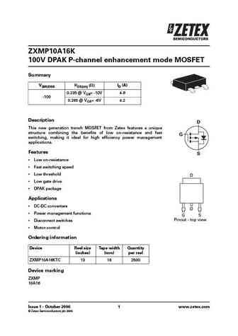
ZXMP10A16K 100V DPAK P-channel enhancement mode MOSFET Summary V(BR)DSS RDS(on) ( ) ID (A) 0.235 @ VGS= -10V 4.6 -100 0.285 @ VGS= -6V 4.2 Description D This new generation trench MOSFET from Zetex features a unique structure combining the benefits of low on-resistance and fast G switching, making it ideal for high efficiency power management applications. Features S Low on-
zxmp10a13fq.pdf
ZXMP10A13FQ 100V P-CHANNEL ENHANCEMENT MODE MOSFET Product Summary Features and Benefits Fast Switching Speed Max ID BVDSS Max RDS(ON) Low Input Capacitance TA = +25 C Low Gate Charge 1.0 @ VGS= -10V -0.7A Low Threshold -100V 1.45 @ VGS= -6.0V -0.5A Totally Lead-Free & Fully RoHS Compliant (Notes 1 & 2) Halogen and Antimony Free.
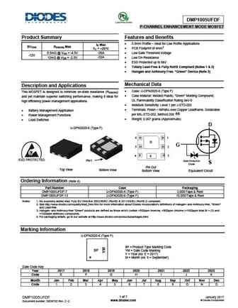
zxmp10a13f.pdf
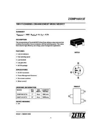
ZXMP10A13F 100V P-CHANNEL ENHANCEMENT MODE MOSFET SUMMARY V(BR)DSS = - 100V RDS(on)= 1 ; ID = - 0.7A DESCRIPTION This new generation of Trench MOSFETs from Zetex utilizes a unique structure that combines the benefits of low on-resistance with fast switching speed. This makes them ideal for high efficiency, low voltage, power management applications. FEATURES SOT23 Low on-resista
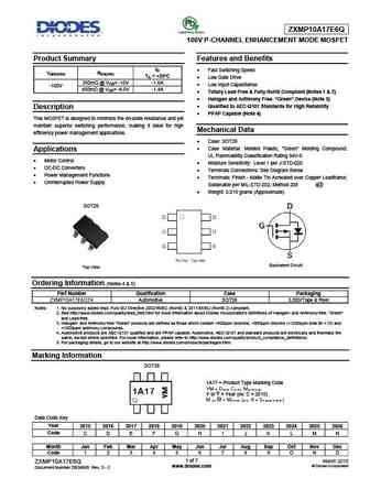
zxmp10a17e6 zxmp10a17e6ta.pdf
A Product Line of Diodes Incorporated ZXMP10A17E6 100V P-CHANNEL ENHANCEMENT MODE MOSFET Please click here to visit our online spice models database. Product Summary Features and Benefits Fast switching speed ID V(BR)DSS RDS(on) Low gate drive TA = 25 C Low input capacitance 350m @ VGS= -10V -1.6 Qualified to AEC-Q101 Standards for High Reliability -1
dmp1009ufdf.pdf
DMP1009UFDF 12V P-CHANNEL ENHANCEMENT MODE MOSFET Product Summary Features 0.6mm Profile Ideal for Low Profile Applications ID max BVDSS RDS(ON) max PCB Footprint of 4mm2 TA = +25 C Low On-Resistance 11m @ VGS = -4.5V -11A Fast Switching Speed Totally Lead-Free & Fully RoHS Compliant (Notes 1 & 2) 14m @ VGS = -3.7V -9.7A -12V Halo
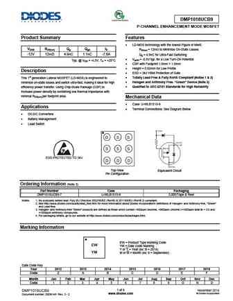
dmp1012ucb9.pdf
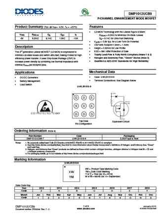
DMP1012UCB9 P-CHANNEL ENHANCEMENT MODE MOSFET Product Summary (Typ. @ VGS = -4.5V, TA = +25 C) Features LD-MOS Technology with the Lowest Figure of Merit VDSS RDS(on) Qg Qgd ID RDS(on) = 8.2m to Minimize On-State Losses -8V 8.2m 8.1nC 1.8nC -10A Qg = 8.1nC for Ultra-Fast Switching Vgs(th) = -0.8V typ. for a Low Turn-On Potential CSP with Footprint 1.5mm 1.
dmp1096ucb4.pdf
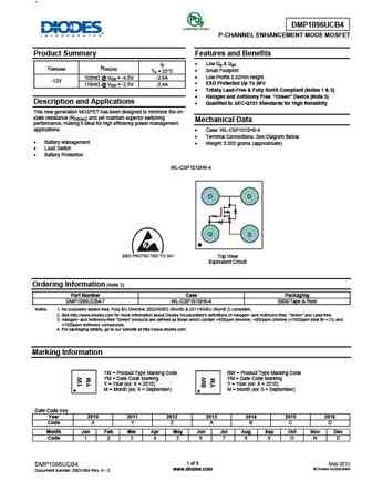
DMP1096UCB4 P-CHANNEL ENHANCEMENT MODE MOSFET Product Summary Features and Benefits Low Qg & Qgd ID V(BR)DSS RDS(ON) Small Footprint TA = 25 C Low Profile 0.62mm height 102m @ VGS = -4.5V -2.6A -12V ESD Protected Up To 3KV 116m @ VGS = -2.5V -2.4A Totally Lead-Free & Fully RoHS Compliant (Notes 1 & 2) Halogen and Antimony Free. Gre
zxmp10a17g.pdf
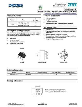
A Product Line of Diodes Incorporated ZXMP10A17G 100V P-CHANNEL ENHANCEMENT MODE MOSFET Please click here to visit our online spice models database. Product Summary Features and Benefits Fast switching speed ID V(BR)DSS RDS(on) Low gate drive TA = 25 C Low input capacitance 350m @ VGS= -10V -2.4 Qualified to AEC-Q101 Standards for High Reliability -10
zxmp10a18gta.pdf
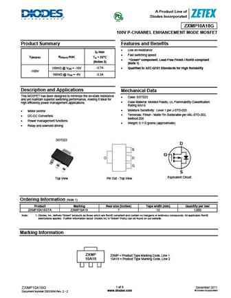
A Product Line of Diodes Incorporated ZXMP10A18G 100V P-CHANNEL ENHANCEMENT MODE MOSFET Product Summary Features and Benefits Low on-resistance ID max Fast switching speed V(BR)DSS RDS(on) max TA = 25 C Green component. Lead Free Finish / RoHS compliant (Notes 3) (Note 1) 150m @ VGS = -10V -3.7A Qualified to AEC-Q101 Standards for High Reliability
dmp1080ucb4.pdf
DMP1080UCB4 P-CHANNEL ENHANCEMENT MODE MOSFET Product Summary (Typ. @ VGS = -4.5V, TA = +25 C) Features LD-MOS Technology with the Lowest Figure of Merit VDSS RDS(on) Qg Qgd ID RDS(on) = 65m to Minimize On-State Losses -12V 65m 2.5nC 0.6nC -3.3A Qg = 2.5nC for Ultra-Fast Switching Vgs(th) = -0.6V typ. for a Low Turn-On Potential Description CSP with Footprin
dmp1011ucb9.pdf
DMP1011UCB9 P-CHANNEL ENHANCEMENT MODE MOSFET Product Summary (Typ. @ VGS = -4.5V, TA = +25 C) Features LD-MOS Technology with the Lowest Figure of Merit VDSS RDS(on) Qg Qgd ID RDS(on) = 8.2m to Minimize On-State Losses -8V 8.2m 8.1nC 1.8nC -10A Qg = 8.1nC for Ultra-Fast Switching Vgs(th) = -0.8V typ. for a Low Turn-On Potential CSP with Footprint 1.5mm 1.5
dmp1045u.pdf
DMP1045U P-CHANNEL ENHANCEMENT MODE MOSFET Product Summary Features and Benefits Low On-Resistance ID BVDSS RDS(ON) Max TA = +25 C Low Input Capacitance Fast Switching Speed 31m @ VGS = -4.5V 5.2A -12V Low Input/Output Leakage 45m @ VGS =-2.5V 4.3A ESD Protected Totally Lead-Free & Fully RoHS Compliant (Notes 1 & 2) Description Ha
dmp1022ufde.pdf
DMP1022UFDE 12V P-CHANNEL ENHANCEMENT MODE MOSFET Product Summary Features 0.6mm profile ideal for low profile applications ID max V(BR)DSS RDS(ON) max PCB footprint of 4mm2 TA = 25 C Low Gate Threshold Voltage Fast Switching Speed 16m @ VGS = -4.5V -9.1A ESD Protected to 3KV 21.5m @ VGS = -2.5V -7.9A Totally Lead-Free & Fully RoHS Comp
dmp1055usw.pdf
DMP1055USW P-CHANNEL ENHANCEMENT MODE MOSFET Product Summary Features Low On-Resistance ID MAX V(BR)DSS RDS(ON) max TA = +25 C Low Gate Threshold Voltage -3.8A 48m @ VGS = -4.5V Low Input Capacitance -12V -3.4A 59m @ VGS = -2.5V Fast Switching Speed 80m @ VGS = -1.8V -2.9A Small Surface Mount Package ESD Protected Description
dmp1046ufdb.pdf
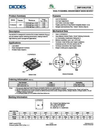
DMP1046UFDB DUAL P-CHANNEL ENHANCEMENT MODE MOSFET Product Summary Features Low On-Resistance ID MAX Device V(BR)DSS RDS(ON) max TA = +25 C Low Input Capacitance Low Profile, 0.6mm Max Height 61m @ VGS = -4.5V -3.8A P-Channel -12V 81m @ VGS = -2.5V -3.3A Totally Lead-Free & Fully RoHS Compliant (Notes 1 & 2) 115m @ VGS = -1.8V -2.8A Halogen and
dmp1018ucb9.pdf
DMP1018UCB9 P-CHANNEL ENHANCEMENT MODE MOSFET Product Summary Features LD-MOS technology with the lowest Figure of Merit VDSS RDS(on) Qg Qgd ID RDS(on) = 12m to Minimize On-State Losses -12V 12m 4.9nC 1.1nC -7.6A Qg = 4.9nC for Ultra-Fast Switching Vgs(th) = -0.8V typ. for a Low Turn-On Potential Typ. @ VGS = -4.5V, TA = +25 C CSP with Footprint 1.5mm 1.5
zxmp10a17e6q.pdf
ZXMP10A17E6Q 100V P-CHANNEL ENHANCEMENT MODE MOSFET Product Summary Features and Benefits ID Fast Switching Speed V(BR)DSS RDS(ON) TA = +25 C Low Gate Drive 350m @ VGS= -10V -1.6A Low Input Capacitance -100V 450m @ VGS= -6.0V -1.4A Totally Lead-Free & Fully RoHS Compliant (Notes 1 & 2) Halogen and Antimony Free. Green Device (Note 3)
zxmp10a17k.pdf
A Product Line of Diodes Incorporated ZXMP10A17K 100V P-CHANNEL ENHANCEMENT MODE MOSFET Please click here to visit our online spice models database. Product Summary Features and Benefits Fast switching speed ID V(BR)DSS RDS(on) Low gate drive TA = 25 C Low input capacitance 350m @ VGS= -10V -3.9A Qualified to AEC-Q101 Standards for High Reliability -1
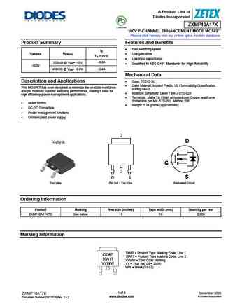
dmp10h400seq.pdf
DMP10H400SEQ 100V P-CHANNEL ENHANCEMENT MODE MOSFET Product Summary Features and Benefits ID Low Gate Drive BVDSS RDS(ON) Max TA = +25 C Low Input Capacitance Fast Switching Speed 250m @ VGS = -10V -2.3A -100V Totally Lead-Free & Fully RoHS Compliant (Notes 1 & 2) 300m @ VGS = -4.5V -2.1A Halogen and Antimony Free. Green Device (Note 3)
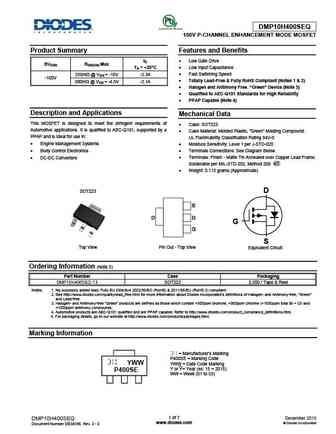
zxmp10a17e6.pdf
ZXMP10A17E6 100V P-CHANNEL ENHANCEMENT MODE MOSFET Product Summary Features and Benefits ID Fast Switching Speed V(BR)DSS RDS(on) TA = +25 C Low Gate Drive 350m @ VGS= -10V -1.6A Low Input Capacitance -100V 450m @ VGS= -6V -1.4A Totally Lead-Free & Fully RoHS Compliant (Notes 1 & 2) Halogen and Antimony Free. Green Device (Note 3) Q
fmp10n60e.pdf
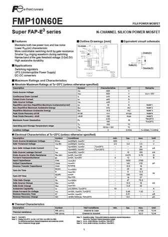
FMP10N60E FUJI POWER MOSFET Super FAP-E3 series N-CHANNEL SILICON POWER MOSFET Features Outline Drawings [mm] Equivalent circuit schematic Maintains both low power loss and low noise TO-220AB Lower R (on) characteristic DS More controllable switching dv/dt by gate resistance Drain(D) Smaller V ringing waveform during switching GS Narrow band of the gate threshold voltage (3.0 0.5V)
mp10n50ei.pdf
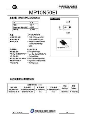
N N- CHANNEL MOSFET R MP10N50EI MAIN CHARACTERISTICS Package ID 10 A VDSS 500 V Rdson-max @Vgs=10V 0.70 Qg-typ 34.38nC APPLICATIONS High efficiency switch mode power supplies - Electronic lamp ballasts UPS based on half bridge
mp10n60eif mp10n60eib mp10n60eis mp10n60eic.pdf
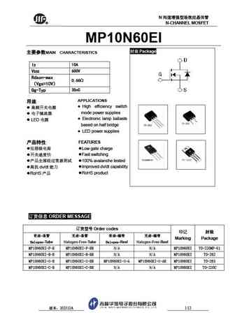
N R N-CHANNEL MOSFET MP10N60EI Package MAIN CHARACTERISTICS ID 10A VDSS 600V Rdson-max 0.66 Vgs=10V Qg-Typ 35nC APPLICATIONS High efficiency switch mode power supplies Electronic lamp ballasts LED based on half bridge LE
dmp1045u.pdf
Product specification DMP1045U P-CHANNEL ENHANCEMENT MODE MOSFET Product Summary Features and Benefits Low On-Resistance ID Low Input Capacitance V(BR)DSS RDS(on) max TA = 25 C Fast Switching Speed Low Input/Output Leakage 31m @ VGS = -4.5V 5.2A Lead Free By Design/RoHS Compliant (Note 1) -12V 4.3A 45m @ VGS =-2.5V ESD Protected Up To
tmp10n80 tmpf10n80.pdf
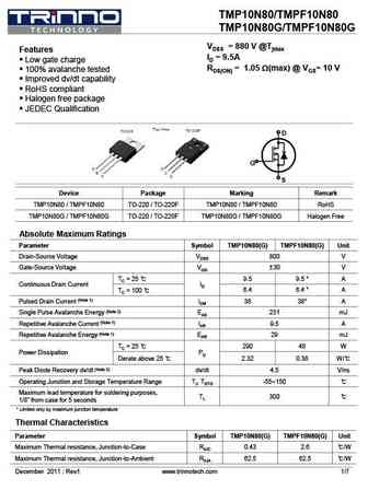
TMP10N80/TMPF10N80 TMP10N80G/TMPF10N80G VDSS = 880 V @Tjmax Features ID = 9.5A Low gate charge RDS(ON) = 1.05 W(max) @ VGS= 10 V 100% avalanche tested Improved dv/dt capability RoHS compliant Halogen free package JEDEC Qualification D G S Device Package Marking Remark TMP10N80 / TMPF10N80 TO-220 / TO-220F TMP10N80 / TMPF10N80 RoHS TMP10N
tmp10n60a tmpf10n60a.pdf
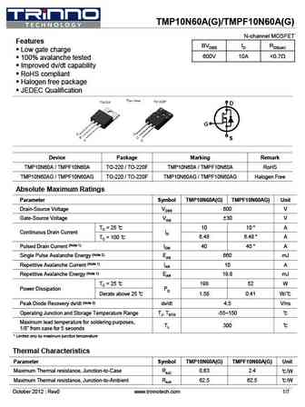
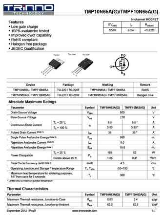
TMP10N60A(G)/TMPF10N60A(G) N-channel MOSFET Features BVDSS ID RDS(on) Low gate charge 600V 10A
tmp10n60 tmpf10n60.pdf
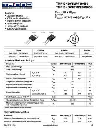
TMP10N60/TMPF10N60 TMP10N60G/TMPF10N60G VDSS = 660 V @Tjmax Features ID = 10A Low gate charge RDS(on) = 0.75 W(max) @ VGS= 10 V 100% avalanche tested Improved dv/dt capability RoHS compliant Halogen free package JEDEC Qualification D G S Device Package Marking Remark TMP10N60 / TMPF10N60 TO-220 / TO-220F TMP10N60 / TMPF10N60 RoHS TMP10N60G / TMPF10N60G
tmp10n65 tmpf10n65.pdf
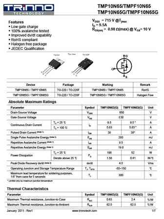
TMP10N65/TMPF10N65 TMP10N65G/TMPF10N65G VDSS = 715 V @Tjmax Features ID = 9.5A Low gate charge RDS(on) = 0.98 W(max) @ VGS= 10 V 100% avalanche tested Improved dv/dt capability RoHS compliant Halogen free package JEDEC Qualification D G S Device Package Marking Remark TMP10N65 / TMPF10N65 TO-220 / TO-220F TMP10N65 / TMPF10N65 RoHS TMP10N
tmp10n65a tmpf10n65a.pdf
TMP10N65A(G)/TMPF10N65A(G) N-channel MOSFET Features BVDSS ID RDS(on) Low gate charge 650V 9.5A
wmm10n65c4 wml10n65c4 wmo10n65c4 wmn10n65c4 wmp10n65c4 wmk10n65c4.pdf

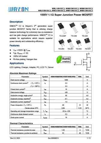
WMM10N65C4, WML10N6 WM C4 65C4, MO10N65C WMN10N65C4, WMP10N6 WM C4 65C4, MK10N65C 650V 0.52 S T V Super Junction Power MOSFET Descrip ption WMOSTM C4 is Wa 4th generation super ayon s n junction MOSFET fa that is utilizing charge M amily S balance te or extremely esistance echnology fo y low on-re D S D G G G S D G and low ga charge performanc WMOSTM
wml10n100c2 wmn10n100c2 wmm10n100c2 wmj10n100c2 wmo10n100c2 wmp10n100c2 wmk10n100c2.pdf
WM 2, WMN10N MM10N100C ML10N100C2 N100C2, WM C2 WMJ10N100C2, WM C2, WMP10N MK10N100C MO10N100C N100C2, WM C2 1000V 1.1 S T 0 Super Junction Power MOSFET Descrip ption WMOSTM C2 is Wa 2nd generation super ayon s n junction MOSFET fa that is utilizing charge M amily S balance te or extremely esistance D echnology fo y low on-re S S G D D G G G and low ga
wml10n105c2 wmn10n105c2 wmm10n105c2 wmj10n105c2 wmo10n105c2 wmp10n105c2 wmk10n105c2.pdf

WM 2, WMN10N MM10N105C ML10N105C2 N105C2, WM C2 WMJ10N105C2, WM C2, WMP10N MK10N105C MO10N105C N105C2, WM C2 1050V 1.1 S T 0 Super Junction Power MOSFET Descrip ption WMOSTM C2 is Wa 2nd generation super ayon s n junction MOSFET fa that is utilizing charge M amily S balance te or extremely esistance D echnology fo y low on-re S S G D D G G G and low ga
wml10n65em wmk10n65em wmm10n65em wmn10n65em wmp10n65em wmo10n65em.pdf

WML10 WMK10N6 0N65EM, W 65EM, WMM10N65EM WMN10 WMP10N6 0N65EM, W 65EM, WMO10N65EM 650V 0.52 S T V Super Junction Power MOSFET Descrip ption WMOSTM EM is Wayon s 3rd generation super W n junction MOSFET fa that is utilizing charge M amily S balance te or extremely esistance echnology fo y low on-re S D D G G G S D G T and low ga ce. WMOSTM EM is ate
wmm10n70c4 wml10n70c4 wmo10n70c4 wmn10n70c4 wmp10n70c4 wmk10n70c4.pdf

WMM10N70C4, WML10N7 WM C4 70C4, MO10N70C WMN10N70C4, WMP10N7 WM C4 70C4, MK10N70C 700V 0.52 S T V Super Junction Power MOSFET Descrip ption WMOSTM C4 is Wa 4th generation super ayon s n junction MOSFET fa that is utilizing charge M amily S balance te or extremely esistance echnology fo y low on-re D S D G G G S D G and low ga charge performanc WMOSTM
wml10n70em wmk10n70em wmm10n70em wmn10n70em wmp10n70em wmo10n70em.pdf

WML10 WMK10N7 0N70EM, W 70EM, WMM10N70EM WMN10 WMP10N7 0N70EM, W 70EM, WMO10N70EM 700V 0.52 S T V Super Junction Power MOSFET Descrip ption WMOSTM EM is Wayon s 3rd generation super W n junction MOSFET fa that is utilizing charge M amily S balance te or extremely esistance echnology fo y low on-re S D D G G G S D G T and low ga ce. WMOSTM EM is ate
wmm10n60c4 wml10n60c4 wmo10n60c4 wmn10n60c4 wmp10n60c4 wmk10n60c4.pdf

WMM10N60C4, WML10N6 WM C4 60C4, MO10N60C WMN10N60C4, WMP10N6 WM C4 60C4, MK10N60C 600V 0.52 S T V Super Junction Power MOSFET Descrip ption WMOSTM C4 is Wa 4th generation super ayon s n junction MOSFET fa that is utilizing charge M amily S balance te or extremely esistance echnology fo y low on-re D S D G G G S D G and low ga charge performanc WMOSTM
wml10n80m3 wmn10n80m3 wmm10n80m3 wmo10n80m3 wmp10n80m3 wmk10n80m3.pdf
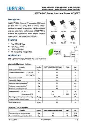
WML10N80M3, W 80M3, WM M3 WMN10N8 MM10N80M WMO1 80M3, WM M3 10N80M3, WMP10N8 MK10N80M 800V 0.86 S T V Super Junction Power MOSFET Descrip ption WMOSTM M3 is Wayo neration 800 M on s 3rd gen 0V super junction MOSFET fa that is utilizing charge M amily S balance te or extremely esistance D echnology fo y low on-re S S G D D G G G T and low ga charge perfo
zxmp10a18ktc.pdf

ZXMP10A18K 100V DPAK P-channel enhancement mode MOSFET Summary V(BR)DSS RDS(on) ( )ID (A) 0.150 @ VGS= -10V -5.9 -100 0.190 @ VGS= -6V -5.2 Description D This new generation trench MOSFET from Zetex features a unique structure combining the benefits of low on-resistance and fast G switching, making it ideal for high efficiency power management applications. Features S Low on
zxmp10a16ktc.pdf

ZXMP10A16K 100V DPAK P-channel enhancement mode MOSFET Summary V(BR)DSS RDS(on) ( ) ID (A) 0.235 @ VGS= -10V 4.6 -100 0.285 @ VGS= -6V 4.2 Description D This new generation trench MOSFET from Zetex features a unique structure combining the benefits of low on-resistance and fast G switching, making it ideal for high efficiency power management applications. Features S Low on-
zxmp10a18k.pdf
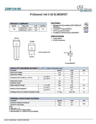
ZXMP10A18K www.VBsemi.tw P-Channel 100 V (D-S) MOSFET FEATURES PRODUCT SUMMARY Halogen-free According to IEC 61249-2-21 VDS (V) RDS(on) ( ) ID (A) Qg (Typ.) Definition 0.250 at VGS = - 10 V - 8.8 TrenchFET Power MOSFET - 100 11.7 0.280 at VGS = - 4.5 V - 8.0 100 % Rg and UIS Tested Compliant to RoHS Directive 2002/95/EC APPLICATIONS TO-251 Power Swit
cmp100n04.pdf
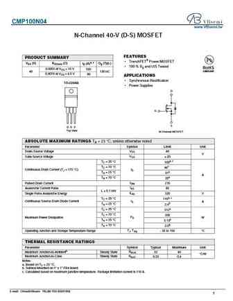
CMP100N04 www.VBsemi.tw N-Channel 40-V (D-S) MOSFET FEATURES PRODUCT SUMMARY TrenchFET Power MOSFET VDS (V) RDS(on) ( ) ID (A)a, c Qg (Typ.) 100 % Rg and UIS Tested RoHS 0.0055 at VGS = 10 V 100 COMPLIANT 40 130 nC 0.0070 at VGS = 4.5 V 90 APPLICATIONS Synchronous Rectification TO-220AB Power Supplies D G S G D S Top View N-Channel MOSFET ABSOLUT
zxmp10a17gta.pdf
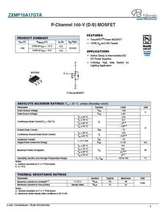
ZXMP10A17GTA www.VBsemi.tw P-Channel 100-V (D-S) MOSFET FEATURES PRODUCT SUMMARY TrenchFET Power MOSFET VDS (V) RDS(on) ( )ID (A) Qg (Typ.) 100% Rg and UIS Tested 0.200 at VGS = - 10 V - 3.0 - 100 13.2 nC 0.230 at VGS = - 6 V - 2.4 APPLICATIONS Available Active Clamp in Intermediate DC/ DC Power Supplies S H-Bridge High Side Switch for Lighting Applicatio
tma10n65h tmp10n65h.pdf
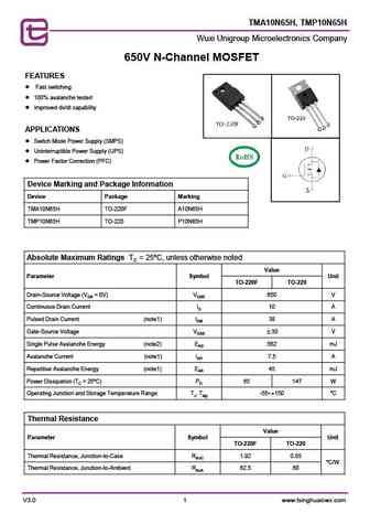
TMA10N65H, TMP10N65H Wuxi Unigroup Microelectronics Company 650V N-Channel MOSFET FEATURES Fast switching 100% avalanche tested Improved dv/dt capability APPLICATIONS Switch Mode Power Supply (SMPS) Uninterruptible Power Supply (UPS) Power Factor Correction (PFC) Device Marking and Package Information Device Package Marking TMA10N65H TO-220F A1
dmp10h400sk3.pdf
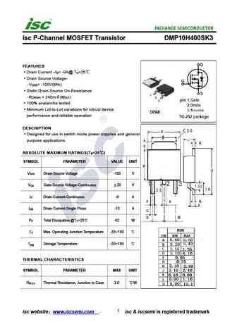
isc P-Channel MOSFET Transistor DMP10H400SK3 FEATURES Drain Current I = -9A@ T =25 D C Drain Source Voltage- V = -100V(Min) DSS Static Drain-Source On-Resistance R = 240m (Max) DS(on) 100% avalanche tested Minimum Lot-to-Lot variations for robust device performance and reliable operation DESCRIPTION Designed for use in switch mode power supplies and general
Otros transistores... MN29, MN32, MN48, MN49, MO810, MO816, MO818, MO870, BC558, MP101, MP101A, MP101B, MP102, MP103, MP103A, MP104, MP1077
History: MP102
🌐 : EN ES РУ

Liste
Recientemente añadidas las descripciónes de los transistores:
BJT: GA1A4M | SBT42 | 2SA200-Y | 2SA200-O | 2SD882-Q | 2SD882-P | 2SD882-E | 2SC945-L | 2SC945-H | 2SC4226-R23 | 2SC3357-F | 2SC3357-E | 2SC3356-R26 | 2SC3356-R24 | 2SC3356-R23 | 2SB772-Q | 2SB772-P | 2SB772-E | 2SA1015-L | 2SA1015-H | HSS8550
Popular searches
a970 | d2390 transistor | 2n5087 equivalent | tip147 datasheet | 2n4124 | mj15022 | toshiba c5198 | irf520n datasheet