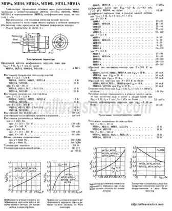
MP10 Specs and Replacement
Type Designator: MP10
Material of Transistor: Ge
Polarity: NPN
Absolute Maximum Ratings
Maximum Collector Power Dissipation (Pc): 0.15 W
Maximum Collector-Base Voltage |Vcb|: 15 V
Maximum Collector-Emitter Voltage |Vce|: 15 V
Maximum Emitter-Base Voltage |Veb|: 15 V
Maximum Collector Current |Ic max|: 0.02 A
Max. Operating Junction Temperature (Tj): 85 °C
Electrical Characteristics
Transition Frequency (ft): 1 MHz
Collector Capacitance (Cc): 60 pF
Forward Current Transfer Ratio (hFE), MIN: 15
Noise Figure, dB: -
MP10 Substitution
- BJT ⓘ Cross-Reference Search
MP10 datasheet
cmp100n04 cmb100n04 cmi100n04.pdf ![]()
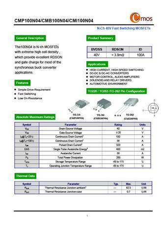
CMP100N04/CMB100N04/CMI100N04 N-Ch 40V Fast Switching MOSFETs General Description Product Summery The100N04 is N-ch MOSFE Ts BVDSS RDSON ID with extreme high cell density , 40V ... See More ⇒
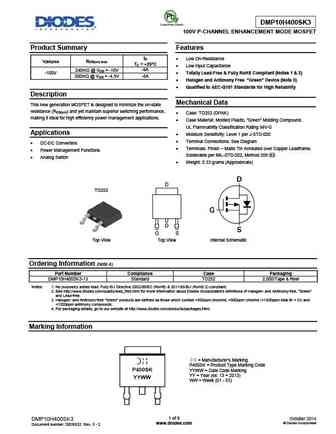
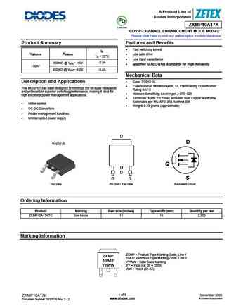
DMP10H400SK3 100V P-CHANNEL ENHANCEMENT MODE MOSFET Product Summary Features ID Low On-Resistance V(BR)DSS RDS(on) max TC = +25 C Low Input Capacitance 240m @ VGS = -10V -9A -100V Totally Lead-Free & Fully RoHS Compliant (Notes 1 & 2) -8A 300m @ VGS = -4.5V Halogen and Antimony Free. Green Device (Note 3) Qualified to AEC-Q101 Standards... See More ⇒
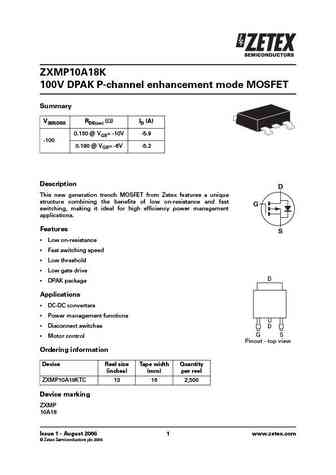
ZXMP10A18K 100V DPAK P-channel enhancement mode MOSFET Summary V(BR)DSS RDS(on) ( )ID (A) 0.150 @ VGS= -10V -5.9 -100 0.190 @ VGS= -6V -5.2 Description D This new generation trench MOSFET from Zetex features a unique structure combining the benefits of low on-resistance and fast G switching, making it ideal for high efficiency power management applications. Features S Low on... See More ⇒
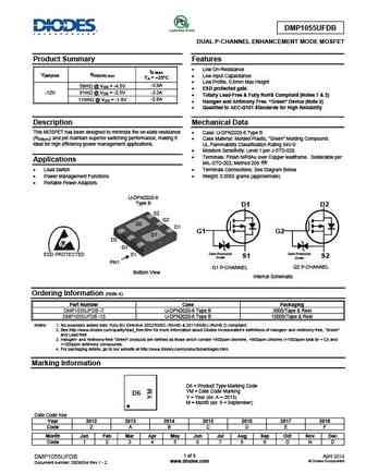
DMP1055UFDB DUAL P-CHANNEL ENHANCEMENT MODE MOSFET Product Summary Features Low On-Resistance ID MAX V(BR)DSS RDS(ON) max Low Input Capacitance TA = +25 C Low Profile, 0.6mm Max Height 59m @ VGS = -4.5V -3.9A ESD protected gate. -12V 81m @ VGS = -2.5V -3.3A Totally Lead-Free & Fully RoHS Compliant (Notes 1 & 2) 115m @ VGS = -1.8V -2.8A ... See More ⇒
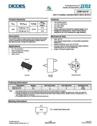
A Product Line of Diodes Incorporated ZXMP10A13F 100V P-CHANNEL ENHANCEMENT MODE MOSFET Product Summary Features Fast Switching Speed Max ID BVDSS Max RDS(ON) Package TA = +25 C Low Input Capacitance Note 5 Low Gate Charge Low Threshold 1.0 @ VGS= -10V -0.7A Totally Lead-Free & Fully RoHS Compliant (Notes 1 & 2) -100V SOT23 Halogen and Antim... See More ⇒
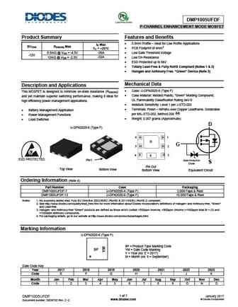
DMP1005UFDF P-CHANNEL ENHANCEMENT MODE MOSFET Product Summary Features and Benefits 0.6mm Profile Ideal for Low Profile Applications ID Max BVDSS RDS(ON) Max PCB Footprint of 4mm2 TC = +25 C 8.5m @ VGS = -4.5V -26A Low Gate Threshold Voltage -12V -22A 12m @ VGS = -2.5V Low On-Resistance ESD Protected up to 8kV Totally Lead-Free & ... See More ⇒
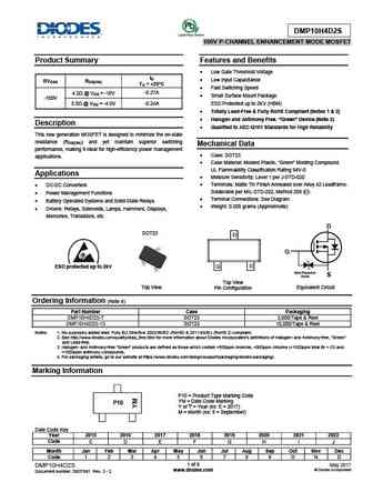
DMP10H4D2S 100V P-CHANNEL ENHANCEMENT MODE MOSFET Product Summary Features and Benefits Low Gate Threshold Voltage ID Low Input Capacitance BVDSS RDS(ON) TA = +25 C Fast Switching Speed 4.2 @ VGS = -10V -0.27A Small Surface Mount Package -100V 5.0 @ VGS = -4.0V -0.24A ESD Protected up to 2KV (HBM) Totally Lead-Free & Fully RoHS Compliant ... See More ⇒
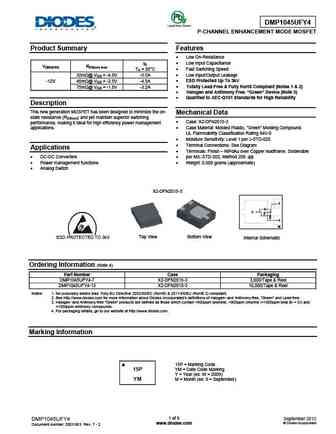
DMP1045UFY4 P-CHANNEL ENHANCEMENT MODE MOSFET Product Summary Features Low On-Resistance ID Low Input Capacitance V(BR)DSS RDS(on) max TA = 25 C Fast Switching Speed 32m @ VGS = -4.5V -5.5A Low Input/Output Leakage -12V 45m @ VGS = -2.5V -4.5A ESD Protected Up To 3kV Totally Lead-Free & Fully RoHS Compliant (Notes 1 & 2) 75m @ VGS = -1.8V -3.2A... See More ⇒
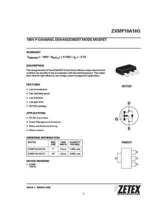
ZXMP10A18G 100V P-CHANNEL ENHANCEMENT MODE MOSFET SUMMARY V(BR)DSS = - 100V RDS(on) = 0.150 ; ID = - 3.7A DESCRIPTION This new generation of Trench MOSFETs from Zetex utilizes a unique structure that combines the benefits of low on-resistance with fast switching speed. This makes them ideal for high efficiency, low voltage, power management applications. FEATURES SOT223 Low on-r... See More ⇒
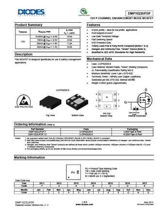
DMP1022UFDF 12V P-CHANNEL ENHANCEMENT MODE MOSFET Product Summary Features ID max 0.6mm profile ideal for low profile applications V(BR)DSS RDS(ON) max TA = +25 C PCB footprint of 4mm2 Low Gate Threshold Voltage 14.8m @ VGS = -4.5V -9.5A Fast Switching Speed 19m @ VGS = -2.5V -8.5A -12V ESD Protected Gate 26m @ VGS = -1.8V -7.2A To... See More ⇒
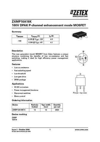
ZXMP10A16K 100V DPAK P-channel enhancement mode MOSFET Summary V(BR)DSS RDS(on) ( ) ID (A) 0.235 @ VGS= -10V 4.6 -100 0.285 @ VGS= -6V 4.2 Description D This new generation trench MOSFET from Zetex features a unique structure combining the benefits of low on-resistance and fast G switching, making it ideal for high efficiency power management applications. Features S Low on-... See More ⇒
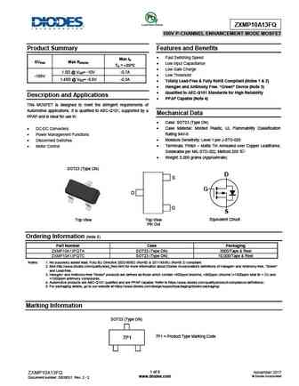
ZXMP10A13FQ 100V P-CHANNEL ENHANCEMENT MODE MOSFET Product Summary Features and Benefits Fast Switching Speed Max ID BVDSS Max RDS(ON) Low Input Capacitance TA = +25 C Low Gate Charge 1.0 @ VGS= -10V -0.7A Low Threshold -100V 1.45 @ VGS= -6.0V -0.5A Totally Lead-Free & Fully RoHS Compliant (Notes 1 & 2) Halogen and Antimony Free. ... See More ⇒
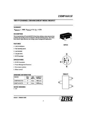
ZXMP10A13F 100V P-CHANNEL ENHANCEMENT MODE MOSFET SUMMARY V(BR)DSS = - 100V RDS(on)= 1 ; ID = - 0.7A DESCRIPTION This new generation of Trench MOSFETs from Zetex utilizes a unique structure that combines the benefits of low on-resistance with fast switching speed. This makes them ideal for high efficiency, low voltage, power management applications. FEATURES SOT23 Low on-resista... See More ⇒
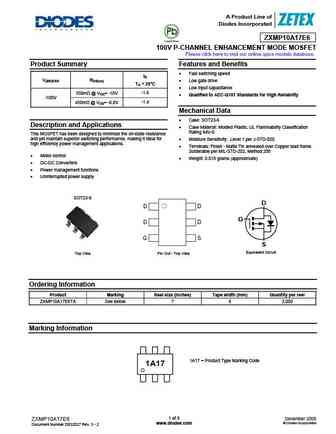
A Product Line of Diodes Incorporated ZXMP10A17E6 100V P-CHANNEL ENHANCEMENT MODE MOSFET Please click here to visit our online spice models database. Product Summary Features and Benefits Fast switching speed ID V(BR)DSS RDS(on) Low gate drive TA = 25 C Low input capacitance 350m @ VGS= -10V -1.6 Qualified to AEC-Q101 Standards for High Reliability -1... See More ⇒
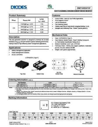
DMP1009UFDF 12V P-CHANNEL ENHANCEMENT MODE MOSFET Product Summary Features 0.6mm Profile Ideal for Low Profile Applications ID max BVDSS RDS(ON) max PCB Footprint of 4mm2 TA = +25 C Low On-Resistance 11m @ VGS = -4.5V -11A Fast Switching Speed Totally Lead-Free & Fully RoHS Compliant (Notes 1 & 2) 14m @ VGS = -3.7V -9.7A -12V Halo... See More ⇒
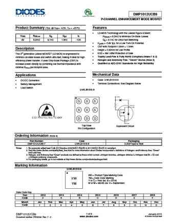
DMP1012UCB9 P-CHANNEL ENHANCEMENT MODE MOSFET Product Summary (Typ. @ VGS = -4.5V, TA = +25 C) Features LD-MOS Technology with the Lowest Figure of Merit VDSS RDS(on) Qg Qgd ID RDS(on) = 8.2m to Minimize On-State Losses -8V 8.2m 8.1nC 1.8nC -10A Qg = 8.1nC for Ultra-Fast Switching Vgs(th) = -0.8V typ. for a Low Turn-On Potential CSP with Footprint 1.5mm 1.... See More ⇒
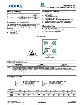
DMP1096UCB4 P-CHANNEL ENHANCEMENT MODE MOSFET Product Summary Features and Benefits Low Qg & Qgd ID V(BR)DSS RDS(ON) Small Footprint TA = 25 C Low Profile 0.62mm height 102m @ VGS = -4.5V -2.6A -12V ESD Protected Up To 3KV 116m @ VGS = -2.5V -2.4A Totally Lead-Free & Fully RoHS Compliant (Notes 1 & 2) Halogen and Antimony Free. Gre... See More ⇒
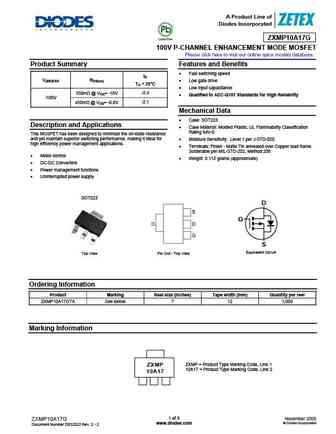
A Product Line of Diodes Incorporated ZXMP10A17G 100V P-CHANNEL ENHANCEMENT MODE MOSFET Please click here to visit our online spice models database. Product Summary Features and Benefits Fast switching speed ID V(BR)DSS RDS(on) Low gate drive TA = 25 C Low input capacitance 350m @ VGS= -10V -2.4 Qualified to AEC-Q101 Standards for High Reliability -10... See More ⇒
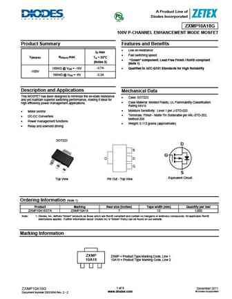
A Product Line of Diodes Incorporated ZXMP10A18G 100V P-CHANNEL ENHANCEMENT MODE MOSFET Product Summary Features and Benefits Low on-resistance ID max Fast switching speed V(BR)DSS RDS(on) max TA = 25 C Green component. Lead Free Finish / RoHS compliant (Notes 3) (Note 1) 150m @ VGS = -10V -3.7A Qualified to AEC-Q101 Standards for High Reliability ... See More ⇒
DMP1080UCB4 P-CHANNEL ENHANCEMENT MODE MOSFET Product Summary (Typ. @ VGS = -4.5V, TA = +25 C) Features LD-MOS Technology with the Lowest Figure of Merit VDSS RDS(on) Qg Qgd ID RDS(on) = 65m to Minimize On-State Losses -12V 65m 2.5nC 0.6nC -3.3A Qg = 2.5nC for Ultra-Fast Switching Vgs(th) = -0.6V typ. for a Low Turn-On Potential Description CSP with Footprin... See More ⇒
DMP1011UCB9 P-CHANNEL ENHANCEMENT MODE MOSFET Product Summary (Typ. @ VGS = -4.5V, TA = +25 C) Features LD-MOS Technology with the Lowest Figure of Merit VDSS RDS(on) Qg Qgd ID RDS(on) = 8.2m to Minimize On-State Losses -8V 8.2m 8.1nC 1.8nC -10A Qg = 8.1nC for Ultra-Fast Switching Vgs(th) = -0.8V typ. for a Low Turn-On Potential CSP with Footprint 1.5mm 1.5... See More ⇒
DMP1045U P-CHANNEL ENHANCEMENT MODE MOSFET Product Summary Features and Benefits Low On-Resistance ID BVDSS RDS(ON) Max TA = +25 C Low Input Capacitance Fast Switching Speed 31m @ VGS = -4.5V 5.2A -12V Low Input/Output Leakage 45m @ VGS =-2.5V 4.3A ESD Protected Totally Lead-Free & Fully RoHS Compliant (Notes 1 & 2) Description Ha... See More ⇒
DMP1022UFDE 12V P-CHANNEL ENHANCEMENT MODE MOSFET Product Summary Features 0.6mm profile ideal for low profile applications ID max V(BR)DSS RDS(ON) max PCB footprint of 4mm2 TA = 25 C Low Gate Threshold Voltage Fast Switching Speed 16m @ VGS = -4.5V -9.1A ESD Protected to 3KV 21.5m @ VGS = -2.5V -7.9A Totally Lead-Free & Fully RoHS Comp... See More ⇒
DMP1055USW P-CHANNEL ENHANCEMENT MODE MOSFET Product Summary Features Low On-Resistance ID MAX V(BR)DSS RDS(ON) max TA = +25 C Low Gate Threshold Voltage -3.8A 48m @ VGS = -4.5V Low Input Capacitance -12V -3.4A 59m @ VGS = -2.5V Fast Switching Speed 80m @ VGS = -1.8V -2.9A Small Surface Mount Package ESD Protected Description ... See More ⇒
DMP1046UFDB DUAL P-CHANNEL ENHANCEMENT MODE MOSFET Product Summary Features Low On-Resistance ID MAX Device V(BR)DSS RDS(ON) max TA = +25 C Low Input Capacitance Low Profile, 0.6mm Max Height 61m @ VGS = -4.5V -3.8A P-Channel -12V 81m @ VGS = -2.5V -3.3A Totally Lead-Free & Fully RoHS Compliant (Notes 1 & 2) 115m @ VGS = -1.8V -2.8A Halogen and ... See More ⇒
DMP1018UCB9 P-CHANNEL ENHANCEMENT MODE MOSFET Product Summary Features LD-MOS technology with the lowest Figure of Merit VDSS RDS(on) Qg Qgd ID RDS(on) = 12m to Minimize On-State Losses -12V 12m 4.9nC 1.1nC -7.6A Qg = 4.9nC for Ultra-Fast Switching Vgs(th) = -0.8V typ. for a Low Turn-On Potential Typ. @ VGS = -4.5V, TA = +25 C CSP with Footprint 1.5mm 1.5... See More ⇒
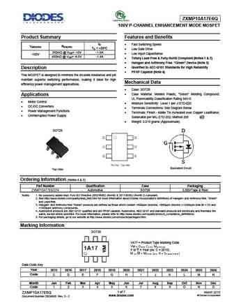
ZXMP10A17E6Q 100V P-CHANNEL ENHANCEMENT MODE MOSFET Product Summary Features and Benefits ID Fast Switching Speed V(BR)DSS RDS(ON) TA = +25 C Low Gate Drive 350m @ VGS= -10V -1.6A Low Input Capacitance -100V 450m @ VGS= -6.0V -1.4A Totally Lead-Free & Fully RoHS Compliant (Notes 1 & 2) Halogen and Antimony Free. Green Device (Note 3) ... See More ⇒
A Product Line of Diodes Incorporated ZXMP10A17K 100V P-CHANNEL ENHANCEMENT MODE MOSFET Please click here to visit our online spice models database. Product Summary Features and Benefits Fast switching speed ID V(BR)DSS RDS(on) Low gate drive TA = 25 C Low input capacitance 350m @ VGS= -10V -3.9A Qualified to AEC-Q101 Standards for High Reliability -1... See More ⇒
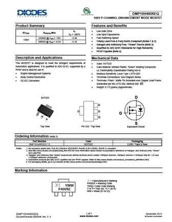
DMP10H400SEQ 100V P-CHANNEL ENHANCEMENT MODE MOSFET Product Summary Features and Benefits ID Low Gate Drive BVDSS RDS(ON) Max TA = +25 C Low Input Capacitance Fast Switching Speed 250m @ VGS = -10V -2.3A -100V Totally Lead-Free & Fully RoHS Compliant (Notes 1 & 2) 300m @ VGS = -4.5V -2.1A Halogen and Antimony Free. Green Device (Note 3) ... See More ⇒
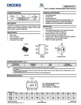
ZXMP10A17E6 100V P-CHANNEL ENHANCEMENT MODE MOSFET Product Summary Features and Benefits ID Fast Switching Speed V(BR)DSS RDS(on) TA = +25 C Low Gate Drive 350m @ VGS= -10V -1.6A Low Input Capacitance -100V 450m @ VGS= -6V -1.4A Totally Lead-Free & Fully RoHS Compliant (Notes 1 & 2) Halogen and Antimony Free. Green Device (Note 3) Q... See More ⇒
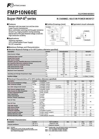
FMP10N60E FUJI POWER MOSFET Super FAP-E3 series N-CHANNEL SILICON POWER MOSFET Features Outline Drawings [mm] Equivalent circuit schematic Maintains both low power loss and low noise TO-220AB Lower R (on) characteristic DS More controllable switching dv/dt by gate resistance Drain(D) Smaller V ringing waveform during switching GS Narrow band of the gate threshold voltage (3.0 0.5V) ... See More ⇒
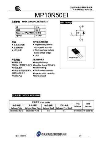
N N- CHANNEL MOSFET R MP10N50EI MAIN CHARACTERISTICS Package ID 10 A VDSS 500 V Rdson-max @Vgs=10V 0.70 Qg-typ 34.38nC APPLICATIONS High efficiency switch mode power supplies - Electronic lamp ballasts UPS based on half bridge ... See More ⇒
mp10n60eif mp10n60eib mp10n60eis mp10n60eic.pdf ![]()
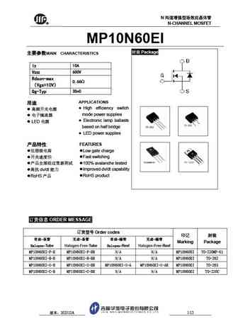
N R N-CHANNEL MOSFET MP10N60EI Package MAIN CHARACTERISTICS ID 10A VDSS 600V Rdson-max 0.66 Vgs=10V Qg-Typ 35nC APPLICATIONS High efficiency switch mode power supplies Electronic lamp ballasts LED based on half bridge LE... See More ⇒
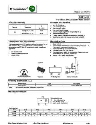
Product specification DMP1045U P-CHANNEL ENHANCEMENT MODE MOSFET Product Summary Features and Benefits Low On-Resistance ID Low Input Capacitance V(BR)DSS RDS(on) max TA = 25 C Fast Switching Speed Low Input/Output Leakage 31m @ VGS = -4.5V 5.2A Lead Free By Design/RoHS Compliant (Note 1) -12V 4.3A 45m @ VGS =-2.5V ESD Protected Up To ... See More ⇒
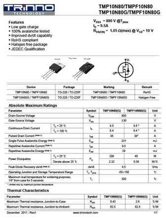
TMP10N80/TMPF10N80 TMP10N80G/TMPF10N80G VDSS = 880 V @Tjmax Features ID = 9.5A Low gate charge RDS(ON) = 1.05 W(max) @ VGS= 10 V 100% avalanche tested Improved dv/dt capability RoHS compliant Halogen free package JEDEC Qualification D G S Device Package Marking Remark TMP10N80 / TMPF10N80 TO-220 / TO-220F TMP10N80 / TMPF10N80 RoHS TMP10N... See More ⇒
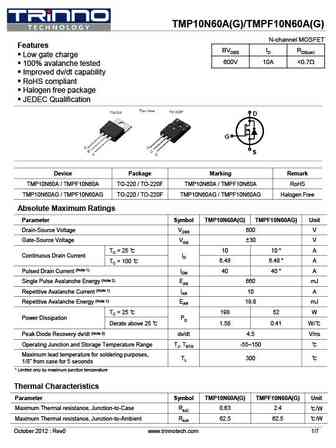
TMP10N60A(G)/TMPF10N60A(G) N-channel MOSFET Features BVDSS ID RDS(on) Low gate charge 600V 10A ... See More ⇒
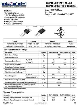
TMP10N60/TMPF10N60 TMP10N60G/TMPF10N60G VDSS = 660 V @Tjmax Features ID = 10A Low gate charge RDS(on) = 0.75 W(max) @ VGS= 10 V 100% avalanche tested Improved dv/dt capability RoHS compliant Halogen free package JEDEC Qualification D G S Device Package Marking Remark TMP10N60 / TMPF10N60 TO-220 / TO-220F TMP10N60 / TMPF10N60 RoHS TMP10N60G / TMPF10N60G... See More ⇒
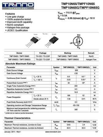
TMP10N65/TMPF10N65 TMP10N65G/TMPF10N65G VDSS = 715 V @Tjmax Features ID = 9.5A Low gate charge RDS(on) = 0.98 W(max) @ VGS= 10 V 100% avalanche tested Improved dv/dt capability RoHS compliant Halogen free package JEDEC Qualification D G S Device Package Marking Remark TMP10N65 / TMPF10N65 TO-220 / TO-220F TMP10N65 / TMPF10N65 RoHS TMP10N... See More ⇒
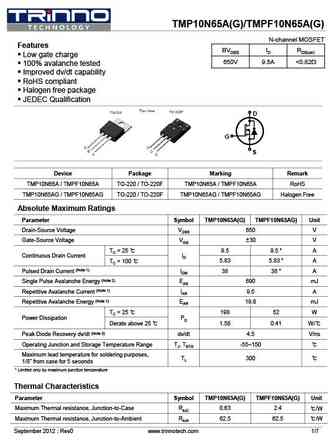
TMP10N65A(G)/TMPF10N65A(G) N-channel MOSFET Features BVDSS ID RDS(on) Low gate charge 650V 9.5A ... See More ⇒
wmm10n65c4 wml10n65c4 wmo10n65c4 wmn10n65c4 wmp10n65c4 wmk10n65c4.pdf ![]()

WMM10N65C4, WML10N6 WM C4 65C4, MO10N65C WMN10N65C4, WMP10N6 WM C4 65C4, MK10N65C 650V 0.52 S T V Super Junction Power MOSFET Descrip ption WMOSTM C4 is Wa 4th generation super ayon s n junction MOSFET fa that is utilizing charge M amily S balance te or extremely esistance echnology fo y low on-re D S D G G G S D G and low ga charge performanc WMOSTM... See More ⇒
wml10n100c2 wmn10n100c2 wmm10n100c2 wmj10n100c2 wmo10n100c2 wmp10n100c2 wmk10n100c2.pdf ![]()
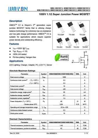
WM 2, WMN10N MM10N100C ML10N100C2 N100C2, WM C2 WMJ10N100C2, WM C2, WMP10N MK10N100C MO10N100C N100C2, WM C2 1000V 1.1 S T 0 Super Junction Power MOSFET Descrip ption WMOSTM C2 is Wa 2nd generation super ayon s n junction MOSFET fa that is utilizing charge M amily S balance te or extremely esistance D echnology fo y low on-re S S G D D G G G and low ga ... See More ⇒
wml10n105c2 wmn10n105c2 wmm10n105c2 wmj10n105c2 wmo10n105c2 wmp10n105c2 wmk10n105c2.pdf ![]()

WM 2, WMN10N MM10N105C ML10N105C2 N105C2, WM C2 WMJ10N105C2, WM C2, WMP10N MK10N105C MO10N105C N105C2, WM C2 1050V 1.1 S T 0 Super Junction Power MOSFET Descrip ption WMOSTM C2 is Wa 2nd generation super ayon s n junction MOSFET fa that is utilizing charge M amily S balance te or extremely esistance D echnology fo y low on-re S S G D D G G G and low ga ... See More ⇒
wml10n65em wmk10n65em wmm10n65em wmn10n65em wmp10n65em wmo10n65em.pdf ![]()

WML10 WMK10N6 0N65EM, W 65EM, WMM10N65EM WMN10 WMP10N6 0N65EM, W 65EM, WMO10N65EM 650V 0.52 S T V Super Junction Power MOSFET Descrip ption WMOSTM EM is Wayon s 3rd generation super W n junction MOSFET fa that is utilizing charge M amily S balance te or extremely esistance echnology fo y low on-re S D D G G G S D G T and low ga ce. WMOSTM EM is ate ... See More ⇒
wmm10n70c4 wml10n70c4 wmo10n70c4 wmn10n70c4 wmp10n70c4 wmk10n70c4.pdf ![]()

WMM10N70C4, WML10N7 WM C4 70C4, MO10N70C WMN10N70C4, WMP10N7 WM C4 70C4, MK10N70C 700V 0.52 S T V Super Junction Power MOSFET Descrip ption WMOSTM C4 is Wa 4th generation super ayon s n junction MOSFET fa that is utilizing charge M amily S balance te or extremely esistance echnology fo y low on-re D S D G G G S D G and low ga charge performanc WMOSTM... See More ⇒
wml10n70em wmk10n70em wmm10n70em wmn10n70em wmp10n70em wmo10n70em.pdf ![]()

WML10 WMK10N7 0N70EM, W 70EM, WMM10N70EM WMN10 WMP10N7 0N70EM, W 70EM, WMO10N70EM 700V 0.52 S T V Super Junction Power MOSFET Descrip ption WMOSTM EM is Wayon s 3rd generation super W n junction MOSFET fa that is utilizing charge M amily S balance te or extremely esistance echnology fo y low on-re S D D G G G S D G T and low ga ce. WMOSTM EM is ate ... See More ⇒
wmm10n60c4 wml10n60c4 wmo10n60c4 wmn10n60c4 wmp10n60c4 wmk10n60c4.pdf ![]()

WMM10N60C4, WML10N6 WM C4 60C4, MO10N60C WMN10N60C4, WMP10N6 WM C4 60C4, MK10N60C 600V 0.52 S T V Super Junction Power MOSFET Descrip ption WMOSTM C4 is Wa 4th generation super ayon s n junction MOSFET fa that is utilizing charge M amily S balance te or extremely esistance echnology fo y low on-re D S D G G G S D G and low ga charge performanc WMOSTM... See More ⇒
wml10n80m3 wmn10n80m3 wmm10n80m3 wmo10n80m3 wmp10n80m3 wmk10n80m3.pdf ![]()
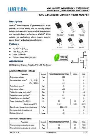
WML10N80M3, W 80M3, WM M3 WMN10N8 MM10N80M WMO1 80M3, WM M3 10N80M3, WMP10N8 MK10N80M 800V 0.86 S T V Super Junction Power MOSFET Descrip ption WMOSTM M3 is Wayo neration 800 M on s 3rd gen 0V super junction MOSFET fa that is utilizing charge M amily S balance te or extremely esistance D echnology fo y low on-re S S G D D G G G T and low ga charge perfo... See More ⇒

ZXMP10A18K 100V DPAK P-channel enhancement mode MOSFET Summary V(BR)DSS RDS(on) ( )ID (A) 0.150 @ VGS= -10V -5.9 -100 0.190 @ VGS= -6V -5.2 Description D This new generation trench MOSFET from Zetex features a unique structure combining the benefits of low on-resistance and fast G switching, making it ideal for high efficiency power management applications. Features S Low on... See More ⇒

ZXMP10A16K 100V DPAK P-channel enhancement mode MOSFET Summary V(BR)DSS RDS(on) ( ) ID (A) 0.235 @ VGS= -10V 4.6 -100 0.285 @ VGS= -6V 4.2 Description D This new generation trench MOSFET from Zetex features a unique structure combining the benefits of low on-resistance and fast G switching, making it ideal for high efficiency power management applications. Features S Low on-... See More ⇒
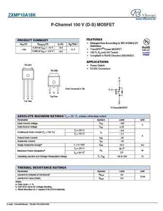
ZXMP10A18K www.VBsemi.tw P-Channel 100 V (D-S) MOSFET FEATURES PRODUCT SUMMARY Halogen-free According to IEC 61249-2-21 VDS (V) RDS(on) ( ) ID (A) Qg (Typ.) Definition 0.250 at VGS = - 10 V - 8.8 TrenchFET Power MOSFET - 100 11.7 0.280 at VGS = - 4.5 V - 8.0 100 % Rg and UIS Tested Compliant to RoHS Directive 2002/95/EC APPLICATIONS TO-251 Power Swit... See More ⇒
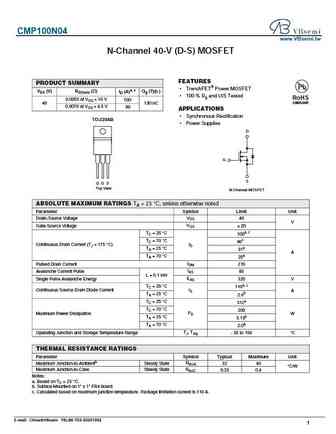
CMP100N04 www.VBsemi.tw N-Channel 40-V (D-S) MOSFET FEATURES PRODUCT SUMMARY TrenchFET Power MOSFET VDS (V) RDS(on) ( ) ID (A)a, c Qg (Typ.) 100 % Rg and UIS Tested RoHS 0.0055 at VGS = 10 V 100 COMPLIANT 40 130 nC 0.0070 at VGS = 4.5 V 90 APPLICATIONS Synchronous Rectification TO-220AB Power Supplies D G S G D S Top View N-Channel MOSFET ABSOLUT... See More ⇒
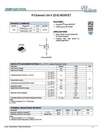
ZXMP10A17GTA www.VBsemi.tw P-Channel 100-V (D-S) MOSFET FEATURES PRODUCT SUMMARY TrenchFET Power MOSFET VDS (V) RDS(on) ( )ID (A) Qg (Typ.) 100% Rg and UIS Tested 0.200 at VGS = - 10 V - 3.0 - 100 13.2 nC 0.230 at VGS = - 6 V - 2.4 APPLICATIONS Available Active Clamp in Intermediate DC/ DC Power Supplies S H-Bridge High Side Switch for Lighting Applicatio... See More ⇒
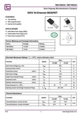
TMA10N65H, TMP10N65H Wuxi Unigroup Microelectronics Company 650V N-Channel MOSFET FEATURES Fast switching 100% avalanche tested Improved dv/dt capability APPLICATIONS Switch Mode Power Supply (SMPS) Uninterruptible Power Supply (UPS) Power Factor Correction (PFC) Device Marking and Package Information Device Package Marking TMA10N65H TO-220F A1... See More ⇒
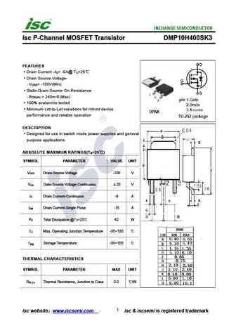
isc P-Channel MOSFET Transistor DMP10H400SK3 FEATURES Drain Current I = -9A@ T =25 D C Drain Source Voltage- V = -100V(Min) DSS Static Drain-Source On-Resistance R = 240m (Max) DS(on) 100% avalanche tested Minimum Lot-to-Lot variations for robust device performance and reliable operation DESCRIPTION Designed for use in switch mode power supplies and general ... See More ⇒
Detailed specifications: MN29, MN32, MN48, MN49, MO810, MO816, MO818, MO870, BC558, MP101, MP101A, MP101B, MP102, MP103, MP103A, MP104, MP1077
Keywords - MP10 pdf specs
MP10 cross reference
MP10 equivalent finder
MP10 pdf lookup
MP10 substitution
MP10 replacement
History: GF121 | MP101 | 2SC2690R | MP102 | MP103A | MP101B | S518T
🌐 : EN ES РУ

LIST
Last Update
BJT: GA1A4M | SBT42 | 2SA200-Y | 2SA200-O | 2SD882-Q | 2SD882-P
Popular searches
a970 | d2390 transistor | 2n5087 equivalent | tip147 datasheet | 2n4124 | mj15022 | toshiba c5198 | irf520n datasheet