MP13 Datasheet. Equivalente. Reemplazo. Hoja de especificaciones. Principales características
Número de Parte: MP13 📄📄
Material: Ge
Polaridad de transistor: NPN
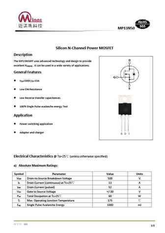
ESPECIFICACIONES MÁXIMAS
Disipación total del dispositivo (Pc): 0.15 W
Tensión colector-base (Vcb): 15 V
Tensión colector-emisor (Vce): 15 V
Tensión emisor-base (Veb): 15 V
Corriente del colector DC máxima (Ic): 0.02 A
Temperatura operativa máxima (Tj): 85 °C
CARACTERÍSTICAS ELÉCTRICAS
Transición de frecuencia (fT): 0.5 MHz
Capacitancia de salida (Cc): 50 pF
Ganancia de corriente contínua (hFE): 12
📄📄 Copiar
Búsqueda de reemplazo de MP13
- Selecciónⓘ de transistores por parámetros
MP13 datasheet
fmp13n60e.pdf
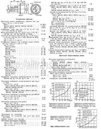
FMP13N60E FUJI POWER MOSFET Super FAP-E3 series N-CHANNEL SILICON POWER MOSFET Features Outline Drawings [mm] Equivalent circuit schematic Maintains both low power loss and low noise TO-220AB Lower R (on) characteristic DS More controllable switching dv/dt by gate resistance Drain(D) Smaller V ringing waveform during switching GS Narrow band of the gate threshold voltage (3.0 0.5V)
fmp13n60es.pdf
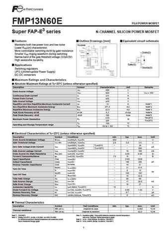
FMP13N60ES FUJI POWER MOSFET Super FAP-E3S series N-CHANNEL SILICON POWER MOSFET Features Outline Drawings [mm] Equivalent circuit schematic Maintains both low power loss and low noise TO-220AB Lower R (on) characteristic DS More controllable switching dv/dt by gate resistance Drain(D) Smaller V ringing waveform during switching GS Narrow band of the gate threshold voltage (4.2 0.5
tmp13n50 tmpf13n50.pdf
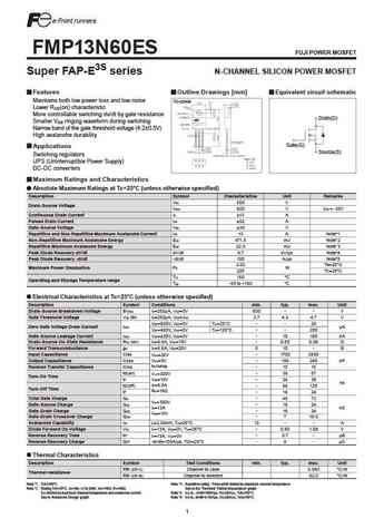
TMP13N50/TMPF13N50 TMP13N50G/TMPF13N50G VDSS = 550 V @Tjmax Features ID = 13A Low gate charge RDS(on) = 0.48 W(max) @ VGS= 10 V 100% avalanche tested Improved dv/dt capability RoHS compliant Halogen free package JEDEC Qualification D G S Device Package Marking Remark TMP13N50 / TMPF13N50 TO-220 / TO-220F TMP13N50 / TMPF13N50 RoHS TMP13N50G / TMPF13N50G

Otros transistores... MP111B, MP112, MP113, MP113A, MP114, MP115, MP116, MP11A, 2SC2383, MP13B, MP14, MP14A, MP14B, MP14I, MP15, MP1529, MP1529A
Parámetros del transistor bipolar y su interrelación.
History: KT837E1-IM | 2N5737 | E7134 | BFV86C | EN915 | 2SA1615-Z | NB024FT
🌐 : EN ES РУ

Liste
Recientemente añadidas las descripciónes de los transistores:
BJT: ZDT6705 | GA1L4Z | GA1A4M | SBT42 | 2SA200-Y | 2SA200-O | 2SD882-Q | 2SD882-P | 2SD882-E | 2SC945-L | 2SC945-H | 2SC4226-R23 | 2SC3357-F | 2SC3357-E | 2SC3356-R26 | 2SC3356-R24 | 2SC3356-R23 | 2SB772-Q | 2SB772-P | 2SB772-E | 2SA1015-L
Popular searches
2n7000 equivalent | tip31 | tip122 transistor | 2sc1079 | 2sc1815 equivalent | 2sa1220 | 2sa940 | 2sc627