MP13 Specs and Replacement
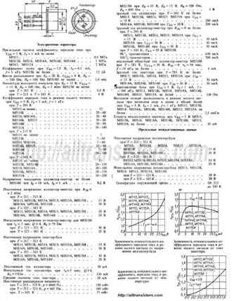
Type Designator: MP13
Material of Transistor: Ge
Polarity: NPN
Absolute Maximum Ratings
Maximum Collector Power Dissipation (Pc): 0.15 W
Maximum Collector-Base Voltage |Vcb|: 15 V
Maximum Collector-Emitter Voltage |Vce|: 15 V
Maximum Emitter-Base Voltage |Veb|: 15 V
Maximum Collector Current |Ic max|: 0.02 A
Max. Operating Junction Temperature (Tj): 85 °C
Electrical Characteristics
Transition Frequency (ft): 0.5 MHz
Collector Capacitance (Cc): 50 pF
Forward Current Transfer Ratio (hFE), MIN: 12
Noise Figure, dB: -
- BJT ⓘ Cross-Reference Search
MP13 datasheet
0.1. Size:466K fuji
fmp13n60e.pdf 

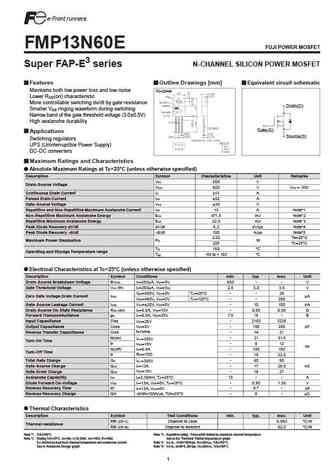
FMP13N60E FUJI POWER MOSFET Super FAP-E3 series N-CHANNEL SILICON POWER MOSFET Features Outline Drawings [mm] Equivalent circuit schematic Maintains both low power loss and low noise TO-220AB Lower R (on) characteristic DS More controllable switching dv/dt by gate resistance Drain(D) Smaller V ringing waveform during switching GS Narrow band of the gate threshold voltage (3.0 0.5V) ... See More ⇒
0.2. Size:528K fuji
fmp13n60es.pdf 

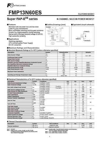
FMP13N60ES FUJI POWER MOSFET Super FAP-E3S series N-CHANNEL SILICON POWER MOSFET Features Outline Drawings [mm] Equivalent circuit schematic Maintains both low power loss and low noise TO-220AB Lower R (on) characteristic DS More controllable switching dv/dt by gate resistance Drain(D) Smaller V ringing waveform during switching GS Narrow band of the gate threshold voltage (4.2 0.5... See More ⇒
0.3. Size:336K trinnotech
tmp13n50 tmpf13n50.pdf 

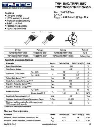
TMP13N50/TMPF13N50 TMP13N50G/TMPF13N50G VDSS = 550 V @Tjmax Features ID = 13A Low gate charge RDS(on) = 0.48 W(max) @ VGS= 10 V 100% avalanche tested Improved dv/dt capability RoHS compliant Halogen free package JEDEC Qualification D G S Device Package Marking Remark TMP13N50 / TMPF13N50 TO-220 / TO-220F TMP13N50 / TMPF13N50 RoHS TMP13N50G / TMPF13N50G... See More ⇒
0.4. Size:658K way-on
wml13n70em wmk13n70em wmm13n70em wmn13n70em wmp13n70em wmo13n70em.pdf 

WML13 WMK13N7 3N70EM, W 70EM, WMM13N70EM WMN13 WMP13N7 3N70EM, W 70EM, WMO13N70EM 700V n Power MOSFET V 0.35 Super Junction Descrip ption WMOSTM EM is Wayon s 3rd generation super W n junction MOSFET fa that is utilizing charge M amily S balance te or extremely esistance echnology fo y low on-re S D D G G G S D G T and low ga ce. WMOSTM EM is ate ch... See More ⇒
0.5. Size:672K way-on
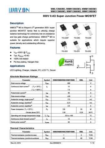
wml13n80m3 wmn13n80m3 wmm13n80m3 wmo13n80m3 wmp13n80m3 wmk13n80m3.pdf 

WML13N80M3, W 80M3, WM M3 WMN13N8 MM13N80M WMO1 80M3, WM M3 13N80M3, WMP13N8 MK13N80M 800V 0.4 S T Super Junction Power MOSFET Descrip ption WMOSTM M3 is Wayo neration 800 M on s 3rd gen 0V super junction MOSFET fa that is utilizing charge M amily S balance te or extremely esistance D echnology fo y low on-re S S G D D G G G T and low ga charge performa... See More ⇒
0.6. Size:661K way-on
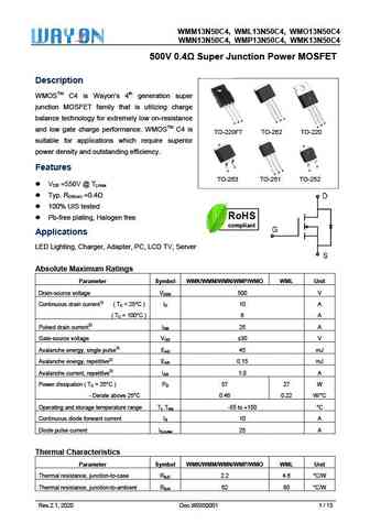
wmm13n50c4 wml13n50c4 wmo13n50c4 wmn13n50c4 wmp13n50c4 wmk13n50c4.pdf 

WMM13N50C4, WML13N5 WM C4 50C4, MO13N50C WMN13N50C4, WMP13N5 WM C4 50C4, MK13N50C 500V 0.4 S unction Power M T V Super Ju MOSFET Descrip ption WMOSTM C4 is Wa 4th generation super ayon s n junction MOSFET fa that is utilizing charge M amily S balance te or extremely esistance echnology fo y low on-re D S D G G G S D G and low ga charge performanc WMO... See More ⇒
0.7. Size:663K way-on
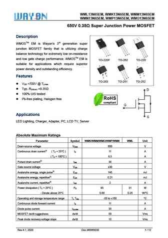
wml13n65em wmk13n65em wmm13n65em wmn13n65em wmp13n65em wmo13n65em.pdf 

WML13 WMK13N6 3N65EM, W 65EM, WMM13N65EM WMN13 WMP13N6 3N65EM, W 65EM, WMO13N65EM 650V n Power MOSFET V 0.35 Super Junction Descrip ption WMOSTM EM is Wayon s 3rd generation super W n junction MOSFET fa that is utilizing charge M amily S balance te or extremely esistance echnology fo y low on-re S D D G G G S D G T and low ga ce. WMOSTM EM is ate ch... See More ⇒
0.8. Size:91K cn minos
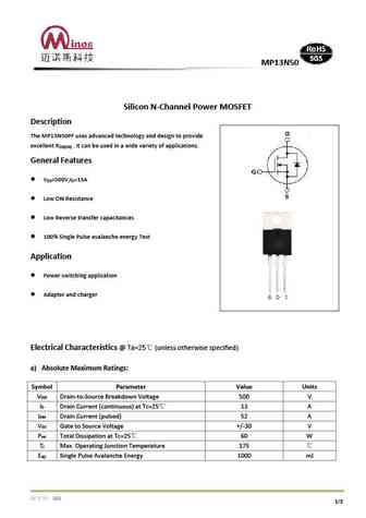
mp13n50.pdf 

MP13N50 SiliconN-Channel Power MOSFET Description TheMP13N50PF uses advancedtechnology anddesigntoprovide excellent R . It canbeusedinawidevariety of applications. DS(ON) General Features V =500V,I =13A DS D LowONResistance LowReversetransfer capacitances 100%SinglePulseavalancheenergy Test Application Power switchingapplication Adapter andcharger Electrical Characteristics... See More ⇒
Detailed specifications: MP111B, MP112, MP113, MP113A, MP114, MP115, MP116, MP11A, 2SC2383, MP13B, MP14, MP14A, MP14B, MP14I, MP15, MP1529, MP1529A
Keywords - MP13 pdf specs
MP13 cross reference
MP13 equivalent finder
MP13 pdf lookup
MP13 substitution
MP13 replacement
