MPS6573 Datasheet. Equivalente. Reemplazo. Hoja de especificaciones. Principales características
Número de Parte: MPS6573 📄📄
Material: Si
Polaridad de transistor: NPN
ESPECIFICACIONES MÁXIMAS
Disipación total del dispositivo (Pc): 0.6 W
Tensión colector-base (Vcb): 35 V
Tensión colector-emisor (Vce): 35 V
Corriente del colector DC máxima (Ic): 0.05 A
Temperatura operativa máxima (Tj): 150 °C
CARACTERÍSTICAS ELÉCTRICAS
Transición de frecuencia (fT): 100 MHz
Capacitancia de salida (Cc): 12 pF
Ganancia de corriente contínua (hFE): 200
Encapsulados: TO92
📄📄 Copiar
Búsqueda de reemplazo de MPS6573
- Selecciónⓘ de transistores por parámetros
MPS6573 datasheet
8.1. Size:279K motorola
mps6571r.pdf 
MOTOROLA Order this document SEMICONDUCTOR TECHNICAL DATA by MPS6571/D Amplifier Transistor NPN Silicon MPS6571 COLLECTOR 3 2 BASE 1 1 2 EMITTER 3 MAXIMUM RATINGS CASE 29 04, STYLE 1 TO 92 (TO 226AA) Rating Symbol Value Unit Collector Emitter Voltage VCEO 20 Vdc Collector Base Voltage VCBO 25 Vdc Emitter Base Voltage VEBO 3.0 Vdc Collector Current Continuous
9.1. Size:173K motorola
mps650re.pdf
MOTOROLA Order this document SEMICONDUCTOR TECHNICAL DATA by MPS650/D NPN Amplifier Transistors MPS650 * MPS651 COLLECTOR COLLECTOR 3 3 PNP MPS750 2 2 BASE BASE * MPS751 NPN PNP Voltage and current are 1 1 negative for PNP transistors EMITTER EMITTER *Motorola Preferred Devices MAXIMUM RATINGS MPS650 MPS651 MPS750 MPS751 Rating Symbol Unit Collector Emitter Voltage V
9.2. Size:69K motorola
mps6560r.pdf
MOTOROLA Order this document SEMICONDUCTOR TECHNICAL DATA by MPS6560/D Audio Transistor MPS6560 NPN Silicon COLLECTOR 3 2 BASE 1 2 1 3 EMITTER CASE 29 04, STYLE 1 MAXIMUM RATINGS TO 92 (TO 226AA) Rating Symbol Value Unit Collector Emitter Voltage VCEO 25 Vdc Collector Base Voltage VCBO 25 Vdc Emitter Base Voltage VEBO 5.0 Vdc Collector Current Continuous I
9.3. Size:59K motorola
mps6507r.pdf
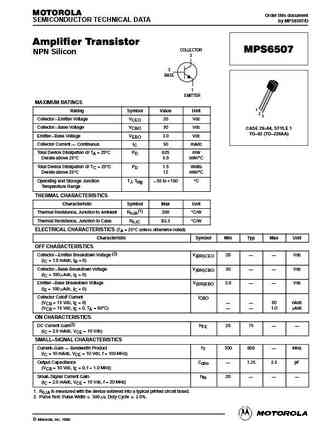
MOTOROLA Order this document SEMICONDUCTOR TECHNICAL DATA by MPS6507/D Amplifier Transistor COLLECTOR MPS6507 NPN Silicon 3 2 BASE 1 EMITTER MAXIMUM RATINGS 1 Rating Symbol Value Unit 2 3 Collector Emitter Voltage VCEO 20 Vdc Collector Base Voltage VCBO 30 Vdc CASE 29 04, STYLE 1 TO 92 (TO 226AA) Emitter Base Voltage VEBO 3.0 Vdc Collector Current Continuo
9.4. Size:304K motorola
mps6530r.pdf
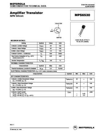
MOTOROLA Order this document SEMICONDUCTOR TECHNICAL DATA by MPS6530/D Amplifier Transistor MPS6530 NPN Silicon COLLECTOR 3 2 BASE 1 2 1 3 EMITTER CASE 29 04, STYLE 1 MAXIMUM RATINGS TO 92 (TO 226AA) Rating Symbol Value Unit Collector Emitter Voltage VCEO 40 Vdc Collector Base Voltage VCBO 60 Vdc Emitter Base Voltage VEBO 5.0 Vdc Collector Current Continuo
9.5. Size:551K motorola
mps6521rev0.pdf
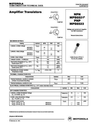
MOTOROLA Order this document SEMICONDUCTOR TECHNICAL DATA by MPS6521/D COLLECTOR 3 Amplifier Transistors NPN 2 BASE * MPS6521 PNP 1 EMITTER MPS6523 COLLECTOR 3 Voltage and current are negative for PNP transistors 2 BASE *Motorola Preferred Device 1 EMITTER MAXIMUM RATINGS Rating Symbol NPN PNP Unit Collector Emitter Voltage VCEO Vdc MPS6521 25 MPS6523 25 C
9.6. Size:791K motorola
mps6520r.pdf
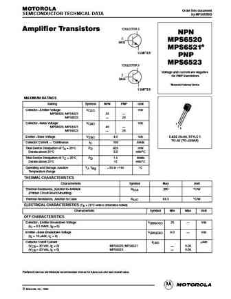
MOTOROLA Order this document SEMICONDUCTOR TECHNICAL DATA by MPS6520/D COLLECTOR 3 Amplifier Transistors NPN 2 MPS6520 BASE * MPS6521 1 EMITTER PNP MPS6523 COLLECTOR 3 Voltage and current are negative 2 for PNP transistors BASE *Motorola Preferred Device 1 EMITTER MAXIMUM RATINGS Rating Symbol NPN PNP Unit Collector Emitter Voltage VCEO Vdc MPS6520, MPS6521 25
9.7. Size:103K fairchild semi
mmbt6515 mps6515.pdf
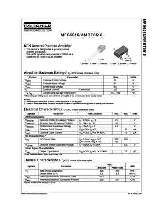
MPS6515/MMBT6515 NPN General Purpose Amplifier 3 This device is designed as a general purpose amplifier and switch. The useful dynamic range extends to 100mA as a 2 switch and to 100MHz as an amplifier. SOT-23 TO-92 1 Mark 3J 1 1. Emitter 2. Base 3. Collector 1. Base 2. Emitter 3. Collector Absolute Maximum Ratings* TC=25 C unless otherwise noted Symbol Parameter Valu
9.8. Size:292K fairchild semi
mps6518.pdf
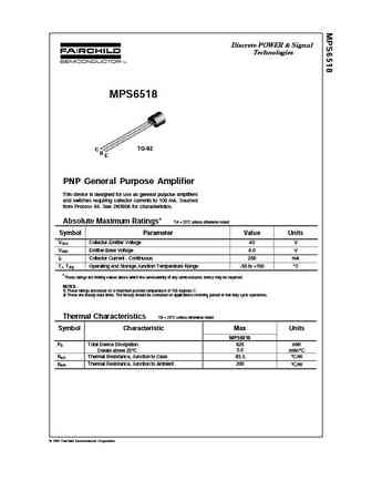
Discrete POWER & Signal Technologies MPS6518 C TO-92 B E PNP General Purpose Amplifier This device is designed for use as general purpose amplifiers and switches requiring collector currents to 100 mA. Sourced from Process 66. See 2N3906 for characteristics. Absolute Maximum Ratings* TA = 25 C unless otherwise noted Symbol Parameter Value Units VCEO Collector-Emitter Voltage 40 V
9.9. Size:293K fairchild semi
mps6562.pdf

Discrete POWER & Signal Technologies MPS6562 C TO-92 B E PNP General Purpose Amplifier This device is designed for use as general purpose amplifiers and switches requiring collector currents to 500 mA. Sourced from Process 67. See TN4033A for characteristics. Absolute Maximum Ratings* TA = 25 C unless otherwise noted Symbol Parameter Value Units VCEO Collector-Emitter Voltage 25 V
9.10. Size:292K fairchild semi
mps6523.pdf

Discrete POWER & Signal Technologies MPS6523 C TO-92 B E PNP General Purpose Amplifier This device is designed for use as general purpose amplifiers and switches requiring collector currents to 300 mA. Sourced from Process 68. See PN200 for characteristics. Absolute Maximum Ratings* TA = 25 C unless otherwise noted Symbol Parameter Value Units VCEO Collector-Emitter Voltage 25 V V
9.11. Size:57K fairchild semi
mps651.pdf
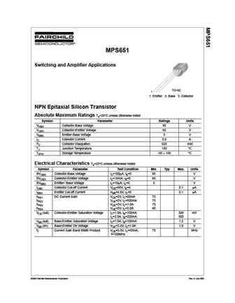
MPS651 Switching and Amplifier Applications TO-92 1 1. Emitter 2. Base 3. Collector NPN Epitaxial Silicon Transistor Absolute Maximum Ratings Ta=25 C unless otherwise noted Symbol Parameter Ratings Units VCBO Collector-Base Voltage 80 V VCEO Collector-Emitter Voltage 60 V VEBO Emitter-Base Voltage 5 V IC Collector Current 0.8 A PC Collector Dissipation 625 mW TJ Junction Temperat
9.12. Size:292K fairchild semi
mps6531.pdf
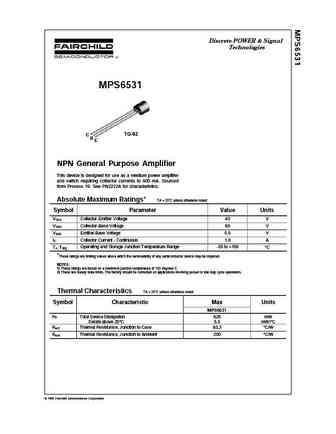
Discrete POWER & Signal Technologies MPS6531 C TO-92 B E NPN General Purpose Amplifier This device is designed for use as a medium power amplifier and switch requiring collector currents to 500 mA. Sourced from Process 19. See PN2222A for characteristics. Absolute Maximum Ratings* TA = 25 C unless otherwise noted Symbol Parameter Value Units VCEO Collector-Emitter Voltage 40 V V C
9.13. Size:126K fairchild semi
mps6513.pdf
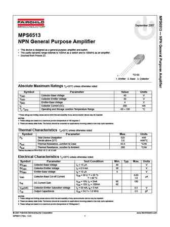
September 2007 MPS6513 NPN General Purpose Amplifier This device is designed as a general purpose amplifier and switch. The useful dynamic range extends to 100mA as a switch and to 100MHz as an amplifier. Sourced from Proces 23. TO-92 1 1. Emitter 2. Base 3. Collector Absolute Maximum Ratings TC=25 C unless otherwise noted Symbol Parameter Value Units VCBO Collector-Ba
9.14. Size:25K fairchild semi
mps6521.pdf
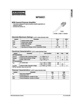
MPS6521 NPN General Purpose Amplifier This device is deisgned for general purpose amplifier applications at collector to 300mA. Sourced from process 10. TO-92 1 1. Emitter 2. Base 3. Collector Absolute Maximum Ratings Ta=25 C unless otherwise noted Symbol Parameter Value Units VCEO Collector-Emitter Voltage 25 V VCBO Collector-Base Voltage 40 V VEBO Emitter-Base Voltage 4
9.15. Size:47K fairchild semi
mps6514.pdf
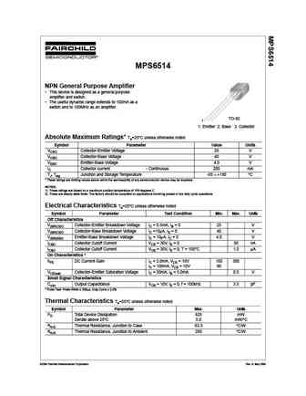
MPS6514 NPN General Purpose Amplifier This device is designed as a general purpose amplifier and switch. The useful dynamic range extends to 100mA as a switch and to 100MHz as an amplifier. TO-92 1 1. Emitter 2. Base 3. Collector Absolute Maximum Ratings* Ta=25 C unless otherwise noted Symbol Parameter Value Units VCEO Collector-Emitter Voltage 25 V VCBO Collector-Base Vo
9.16. Size:292K fairchild semi
mps6534.pdf

Discrete POWER & Signal Technologies MPS6534 C TO-92 B E PNP General Purpose Amplifier This device is designed for use as general purpose amplifiers and switches requiring collector currents to 500 mA. Sourced from Process 63. See PN2907A for characteristics. Absolute Maximum Ratings* TA = 25 C unless otherwise noted Symbol Parameter Value Units VCEO Collector-Emitter Voltage 40 V
9.17. Size:44K central
mps6520-mps6521.pdf
145 Adams Avenue, Hauppauge, NY 11788 USA Tel (631) 435-1110 Fax (631) 435-1824
9.19. Size:111K central
mps651x series.pdf
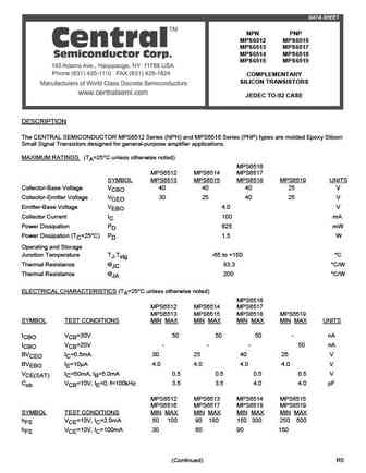
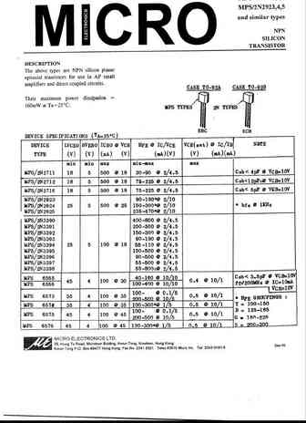
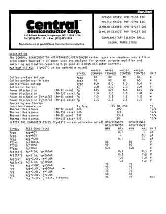
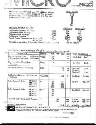
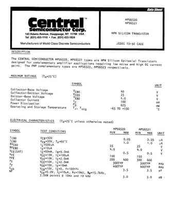
DATA SHEET NPN PNP MPS6512 MPS6516 MPS6513 MPS6517 MPS6514 MPS6518 MPS6515 MPS6519 COMPLEMENTARY SILICON TRANSISTORS JEDEC TO-92 CASE DESCRIPTION The CENTRAL SEMICONDUCTOR MPS6512 Series (NPN) and MPS6516 Series (PNP) types are molded Epoxy Silicon Small Signal Transistors designed for general-purpose amplifier applications. MAXIMUM RATINGS (TA=25 C unless otherwise noted)
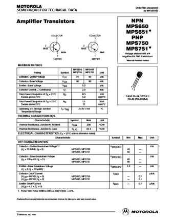
9.20. Size:68K onsemi
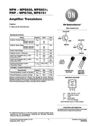
mps650 mps651 mps750 mps751.pdf
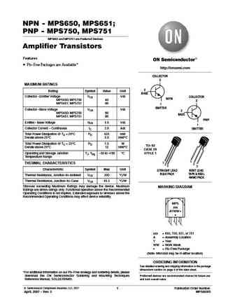
NPN - MPS650, MPS651; PNP - MPS750, MPS751 MPS651 and MPS751 are Preferred Devices Amplifier Transistors Features Pb-Free Packages are Available* http //onsemi.com COLLECTOR 3 MAXIMUM RATINGS 2 Rating Symbol Value Unit BASE Collector-Emitter Voltage VCE Vdc COLLECTOR NPN MPS650; MPS750 40 3 MPS651; MPS751 60 1 EMITTER Collector-Base Voltage VCB Vdc 2 MPS650; MPS750 60
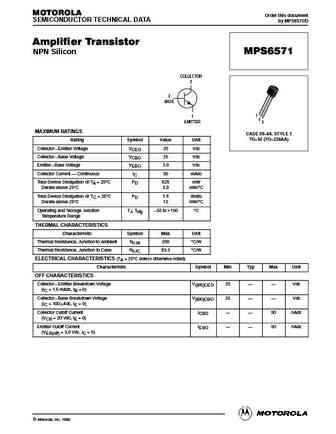
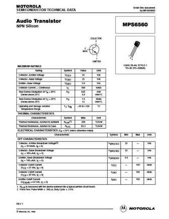
9.21. Size:43K onsemi
mps6560-d.pdf
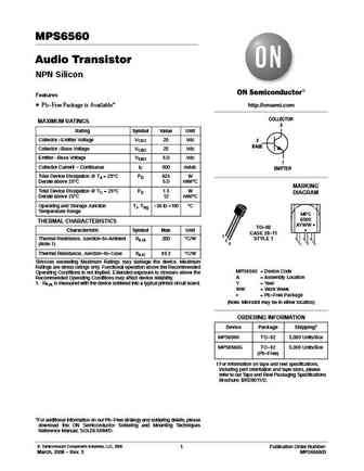
MPS6560 Audio Transistor NPN Silicon Features Pb-Free Package is Available* http //onsemi.com COLLECTOR MAXIMUM RATINGS 3 Rating Symbol Value Unit Collector -Emitter Voltage VCEO 25 Vdc 2 BASE Collector -Base Voltage VCBO 25 Vdc Emitter -Base Voltage VEBO 5.0 Vdc 1 Collector Current - Continuous IC 500 mAdc EMITTER Total Device Dissipation @ TA = 25 C PD 625 W Derate abo
9.22. Size:106K onsemi
mps651rlrmg.pdf

NPN - MPS650, MPS651; PNP - MPS750, MPS751 Amplifier Transistors Features These are Pb-Free Devices* http //onsemi.com COLLECTOR 3 MAXIMUM RATINGS 2 Rating Symbol Value Unit BASE Collector-Emitter Voltage VCE Vdc COLLECTOR NPN MPS650; MPS750 40 3 MPS651; MPS751 60 1 EMITTER Collector-Base Voltage VCB Vdc 2 MPS650; MPS750 60 BASE MPS651; MPS751 80 PNP Emitter-Base V
9.23. Size:166K onsemi
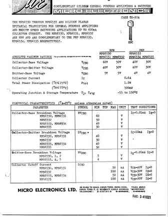
mps6521 mps6523.pdf
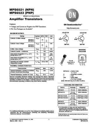
MPS6521 (NPN) MPS6523 (PNP) MPS6521 is a Preferred Device Amplifier Transistors Features Voltage and Current are Negative for PNP Transistors http //onsemi.com Pb-Free Packages are Available* COLLECTOR COLLECTOR MAXIMUM RATINGS 3 3 Rating Symbol NPN PNP Unit 2 2 Collector -Emitter Voltage VCEO Vdc BASE BASE MPS6521 25 - MPS6523 - 25 1 1 Collector -Base Voltage VCB
9.24. Size:106K onsemi
mps651g.pdf
NPN - MPS650, MPS651; PNP - MPS750, MPS751 Amplifier Transistors Features These are Pb-Free Devices* http //onsemi.com COLLECTOR 3 MAXIMUM RATINGS 2 Rating Symbol Value Unit BASE Collector-Emitter Voltage VCE Vdc COLLECTOR NPN MPS650; MPS750 40 3 MPS651; MPS751 60 1 EMITTER Collector-Base Voltage VCB Vdc 2 MPS650; MPS750 60 BASE MPS651; MPS751 80 PNP Emitter-Base V
9.25. Size:217K secos
mps651.pdf
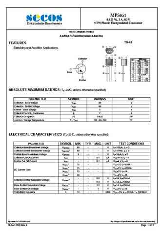
MPS651 0.625 W, 2 A, 60 V NPN Plastic Encapsulated Transistor Elektronische Bauelemente RoHS Compliant Product A suffix of -C specifies halogen & lead-free TO-92 FEATURES G H Switching and Amplifier Applications J A D Collector Millimeter REF. Min. Max. 2 B A 4.40 4.70 B 4.30 4.70 K C 12.70 - D 3.30 3.81 3 E 0.36 0.56 Base F 0.36 0.51 E C F
9.26. Size:250K cdil
mps6530 31.pdf
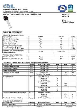
Continental Device India Limited An ISO/TS 16949, ISO 9001 and ISO 14001 Certified Company NPN SILICON PLANAR EPITAXIAL TRANSISTORS MPS6530 MPS6531 TO-92 Plastic Package C B E AMPLIFIER TRANSISTOR ABSOLUTE MAXIMUM RATINGS DESCRIPTION SYMBOL VALUE UNITS VCEO Collector Emitter Voltage 40 V VCBO Collector Base Voltage 60 V VEBO Emitter Base Voltage 5 V IC Collector Current Conti
9.27. Size:191K cdil
mps650 51 mps750 51.pdf
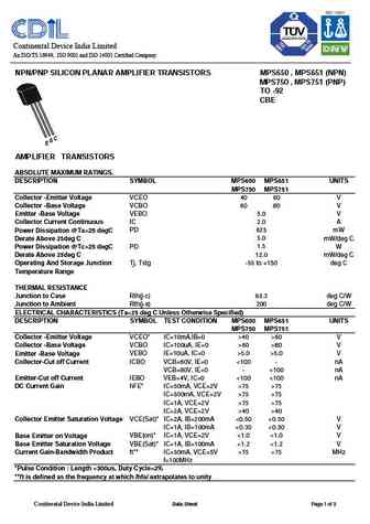
Continental Device India Limited An ISO/TS 16949, ISO 9001 and ISO 14001 Certified Company NPN/PNP SILICON PLANAR AMPLIFIER TRANSISTORS MPS650 , MPS651 (NPN) MPS750 , MPS751 (PNP) TO -92 CBE AMPLIFIER TRANSISTORS ABSOLUTE MAXIMUM RATINGS. DESCRIPTION SYMBOL MPS650 MPS651 UNITS MPS750 MPS751 Collector -Emitter Voltage VCEO 40 60 V Collector -Base Voltage VCBO 60 80 V Emitter -Base Vo
9.28. Size:349K cdil
mps6560-2.pdf
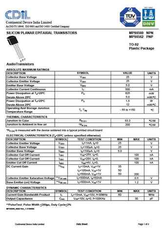
Continental Device India Limited An ISO/TS 16949, ISO 9001 and ISO 14001 Certified Company SILICON PLANAR EPITAXIAL TRANSISTORS MPS6560 NPN MPS6562 PNP TO-92 Plastic Package C B E AudioTransistors ABSOLUTE MAXIMUM RATINGS DESCRIPTION SYMBOL VALUE UNITS VCBO Collector Base Voltage 25 V VCEO Collector Emitter Voltage 25 V VEBO Emitter Base Voltage 5.0 V IC Collector Current Con
9.29. Size:424K jiangsu
mps651.pdf
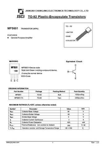
JIANGSU CHANGJING ELECTRONICS TECHNOLOGY CO., LTD TO-92 Plastic-Encapsulate Transistors TO 92 MPS651 TRANSISTOR (NPN) 1.EMITTER FEATURES 2.BASE General Purpose Amplifier 3.COLLECTOR Equivalent Circuit MPS651=Device code MPS651 Solid dot=Green molding compound device, if none,the normal device XXX=Code
9.30. Size:350K kec
mps651.pdf
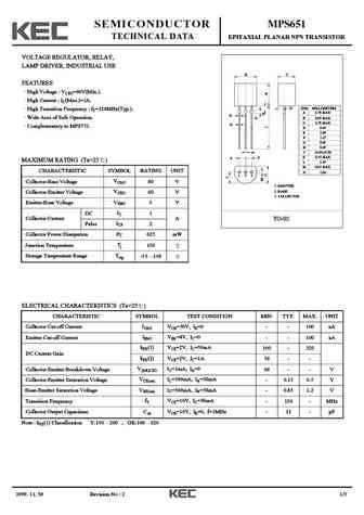
SEMICONDUCTOR MPS651 TECHNICAL DATA EPITAXIAL PLANAR NPN TRANSISTOR VOLTAGE REGULATOR, RELAY, LAMP DRIVER, INDUSTRIAL USE B C FEATURES High Voltage VCEO=60V(Min.). High Current IC(Max.)=1A. N DIM MILLIMETERS High Transition Frequency fT=150MHz(Typ.). A 4.70 MAX E K B 4.80 MAX Wide Area of Safe Operation. G C 3.70 MAX D Complementary to MPS751. D 0.45 E 1.00 F 1.27 G
9.34. Size:159K first silicon
mps651.pdf
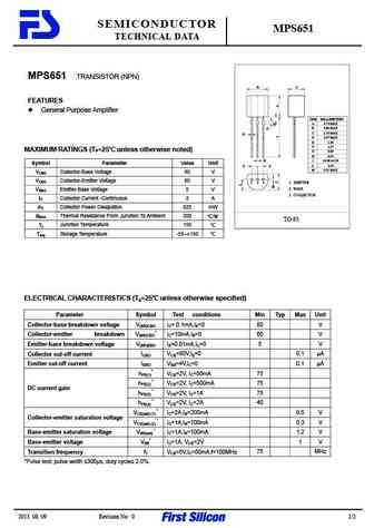
SEMICONDUCTOR MPS651 TECHNICAL DATA MPS651 TRANSISTOR (NPN) B C FEATURES General Purpose Amplifier DIM MILLIMETERS A 4.70 MAX E B 4.80 MAX G C 3.70 MAX D D 0.55 MAX E 1.00 F 1.27 MAXIMUM RATINGS (Ta=25 unless otherwise noted) G 0.85 H 0.45 _ H J 14.00 + 0.50 Symbol Parameter Value Unit L 2.30 F F M 0.51 MAX VCBO Collector-Base Voltage 80 V VCEO Collector-Em
Otros transistores... MPS6568, MPS6568A, MPS6569, MPS6569A, MPS6570, MPS6570A, MPS6571, MPS6572, 2SB649, MPS6574, MPS6575, MPS6576, MPS6579, MPS6580, MPS6590, MPS6591, MPS6595