2N49 Datasheet. Equivalente. Reemplazo. Hoja de especificaciones. Principales características
Número de Parte: 2N49 📄📄
Material: Ge
Polaridad de transistor: PNP
ESPECIFICACIONES MÁXIMAS
Disipación total del dispositivo (Pc): 0.05 W
Tensión colector-base (Vcb): 35 V
Corriente del colector DC máxima (Ic): 0.02 A
Temperatura operativa máxima (Tj): 50 °C
CARACTERÍSTICAS ELÉCTRICAS
Transición de frecuencia (fT): 0.8 MHz
Ganancia de corriente contínua (hFE): 39
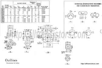
Encapsulados: TO28
📄📄 Copiar
Búsqueda de reemplazo de 2N49
- Selecciónⓘ de transistores por parámetros
2N49 datasheet
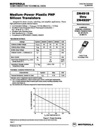
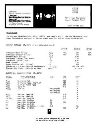
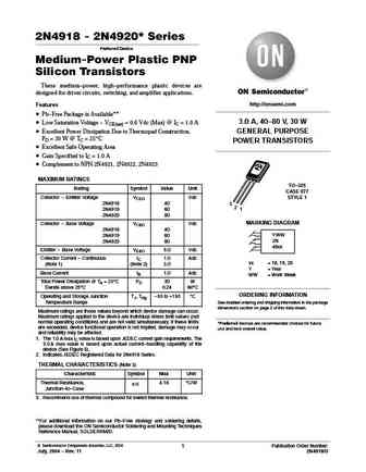
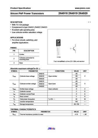
2n4918 2n4919 2n4920.pdf
Order this document MOTOROLA by 2N4918/D SEMICONDUCTOR TECHNICAL DATA 2N4918 Medium-Power Plastic PNP thru Silicon Transistors * 2N4920 . . . designed for driver circuits, switching, and amplifier applications. These high performance plastic devices feature *Motorola Preferred Device Low Saturation Voltage VCE(sat) = 0.6 Vdc (Max) @ IC = 1.0 Amp 3 AMPERE Excellent
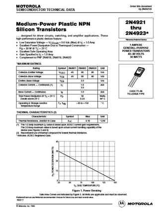
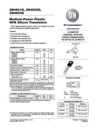
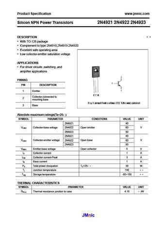
2n4921 2n4922 2n4923.pdf
Order this document MOTOROLA by 2N4921/D SEMICONDUCTOR TECHNICAL DATA 2N4921 Medium-Power Plastic NPN thru Silicon Transistors 2N4923 * . . . designed for driver circuits, switching, and amplifier applications. These high performance plastic devices feature *Motorola Preferred Device Low Saturation Voltage VCE(sat) = 0.6 Vdc (Max) @ IC = 1.0 Amp 1 AMPERE Excellent
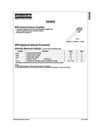
2n4953.pdf
2N4953 NPN General Purpose Amplifier This device designed for use as general purpose amplifier and switches requiring collector currents to 500mA. Sourced from Process 10. TO-92 1 1. Emitter 2. Collector 3. Base NPN Epitaxial Silicon Transistor Absolute Maximum Ratings* Ta=25 C unless otherwise noted Symbol Parameter Value Units VCEO Collector-Emitter Voltage 30 V VCBO C
2n4918 2n4919 2n4920 2.pdf
145 Adams Avenue, Hauppauge, NY 11788 USA Tel (631) 435-1110 Fax (631) 435-1824
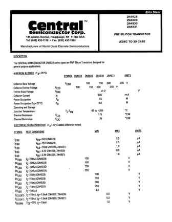
2n4928 2n4929 2n4930 2n4931.pdf
145 Adams Avenue, Hauppauge, NY 11788 USA Tel (631) 435-1110 Fax (631) 435-1824
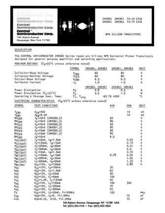
2n4960 2n4961 2n4962 2n4963.pdf
145 Adams Avenue, Hauppauge, NY 11788 USA Tel (631) 435-1110 Fax (631) 435-1824
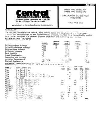
2n4904 2n4905 2n4906 2n4913 2n4914 2n4915.pdf
145 Adams Avenue, Hauppauge, NY 11788 USA Tel (631) 435-1110 Fax (631) 435-1824
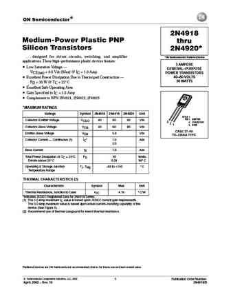
2n4918 2n4919 2n4920.pdf
ON Semiconductor) 2N4918 Medium-Power Plastic PNP thru Silicon Transistors * 2N4920 . . . designed for driver circuits, switching, and amplifier *ON Semiconductor Preferred Device applications. These high performance plastic devices feature 3 AMPERE Low Saturation Voltage GENERAL PURPOSE VCE(sat) = 0.6 Vdc (Max) @ IC = 1.0 Amp POWER TRANSISTORS 40 80 VOLTS Exc
2n4920g9285.pdf
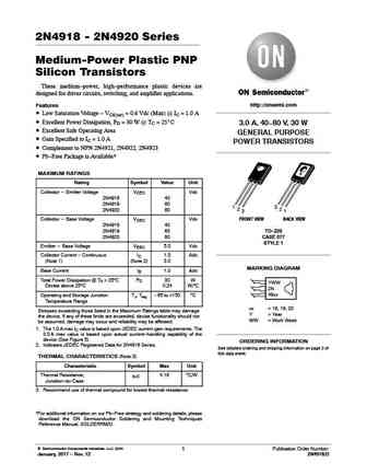
2N4918 - 2N4920* Series Preferred Device Medium-Power Plastic PNP Silicon Transistors These medium-power, high-performance plastic devices are designed for driver circuits, switching, and amplifier applications. http //onsemi.com Features Pb-Free Package is Available** 3.0 A, 40-80 V, 30 W Low Saturation Voltage - VCE(sat) = 0.6 Vdc (Max) @ IC = 1.0 A Excellent Power Dis
2n4918 2n4919 2n4920 2n4920g.pdf
2N4918 - 2N4920 Series Medium-Power Plastic PNP Silicon Transistors These medium-power, high-performance plastic devices are designed for driver circuits, switching, and amplifier applications. http //onsemi.com Features Low Saturation Voltage - VCE(sat) = 0.6 Vdc (Max) @ IC = 1.0 A Excellent Power Dissipation, PD = 30 W @ TC = 25_C 3.0 A, 40-80 V, 30 W Excellent Safe Oper
2n4919g.pdf
2N4918 - 2N4920* Series Preferred Device Medium-Power Plastic PNP Silicon Transistors These medium-power, high-performance plastic devices are designed for driver circuits, switching, and amplifier applications. http //onsemi.com Features Pb-Free Package is Available** 3.0 A, 40-80 V, 30 W Low Saturation Voltage - VCE(sat) = 0.6 Vdc (Max) @ IC = 1.0 A Excellent Power Dis
2n4921g.pdf
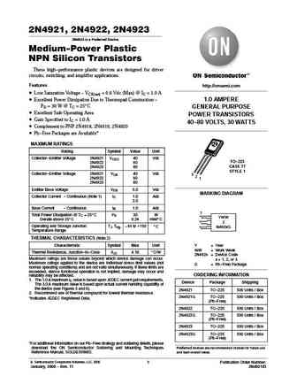
2N4921, 2N4922, 2N4923 2N4923 is a Preferred Device Medium-Power Plastic NPN Silicon Transistors These high-performance plastic devices are designed for driver circuits, switching, and amplifier applications. Features http //onsemi.com Low Saturation Voltage - VCE(sat) = 0.6 Vdc (Max) @ IC = 1.0 A 1.0 AMPERE Excellent Power Dissipation Due to Thermopad Construction - PD = 30
2n4923g.pdf
2N4921, 2N4922, 2N4923 2N4923 is a Preferred Device Medium-Power Plastic NPN Silicon Transistors These high-performance plastic devices are designed for driver circuits, switching, and amplifier applications. Features http //onsemi.com Low Saturation Voltage - VCE(sat) = 0.6 Vdc (Max) @ IC = 1.0 A 1.0 AMPERE Excellent Power Dissipation Due to Thermopad Construction - PD = 30
2n4921 2n4922 2n4923.pdf
2N4921, 2N4922, 2N4923 2N4923 is a Preferred Device Medium-Power Plastic NPN Silicon Transistors These high-performance plastic devices are designed for driver circuits, switching, and amplifier applications. Features http //onsemi.com Low Saturation Voltage - VCE(sat) = 0.6 Vdc (Max) @ IC = 1.0 A 1.0 AMPERE Excellent Power Dissipation Due to Thermopad Construction - PD = 30
2n4918g.pdf
2N4918 - 2N4920* Series Preferred Device Medium-Power Plastic PNP Silicon Transistors These medium-power, high-performance plastic devices are designed for driver circuits, switching, and amplifier applications. http //onsemi.com Features Pb-Free Package is Available** 3.0 A, 40-80 V, 30 W Low Saturation Voltage - VCE(sat) = 0.6 Vdc (Max) @ IC = 1.0 A Excellent Power Dis
2n4922g.pdf
2N4921, 2N4922, 2N4923 2N4923 is a Preferred Device Medium-Power Plastic NPN Silicon Transistors These high-performance plastic devices are designed for driver circuits, switching, and amplifier applications. Features http //onsemi.com Low Saturation Voltage - VCE(sat) = 0.6 Vdc (Max) @ IC = 1.0 A 1.0 AMPERE Excellent Power Dissipation Due to Thermopad Construction - PD = 30
2n4921g 2n4922g 2n4923g.pdf
2N4921G, 2N4922G, 2N4923G Medium-Power Plastic NPN Silicon Transistors These high-performance plastic devices are designed for driver circuits, switching, and amplifier applications. www.onsemi.com Features 1.0 AMPERE Low Saturation Voltage GENERAL PURPOSE Excellent Power Dissipation POWER TRANSISTORS Excellent Safe Operating Area 40-80 VOLTS, 30 WATTS Complement
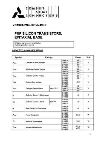
2n4901-2n4902-2n4903.pdf
PNP SILICON TRANSISTORS, PNP SILICON TRANSISTORS, EPITAXIAL BASE EPITAXIAL BASE LF Large signal power amplification Switching medium current ABSOLUTE MAXIMUM RATINGS Symbol Ratings Value Unit 2N4901 -40 VCBO Collector to Base Voltage 2N4902 -60 V 2N4903 -80 2N4901 -40 VCEO #Collector-Emitter Voltage 2N4902 -60 V 2N4903 -80 2N4901 -40 VCER Collector-Emitter Voltage 2
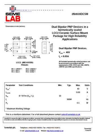
2n4939dcsm.pdf
"2N4938DCSM" 2N4939DCSM Dimensions in mm (inches). Dual Bipolar PNP Devices in a hermetically sealed LCC2 Ceramic Surface Mount Package for High Reliability 1.40 0.15 2.29 0.20 1.65 0.13 (0.055 0.006) (0.09 0.008) (0.065 0.005) Applications 2 3 1 4 Dual Bipolar PNP Devices. A 0.23 6 5 rad. (0.009) V = 40V CEO 6.22 0.13 A = 1.2
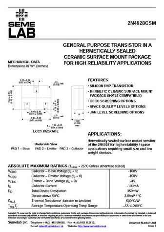
2n4928csm.pdf
2N4928CSM GENERAL PURPOSE TRANSISTOR IN A HERMETICALLY SEALED CERAMIC SURFACE MOUNT PACKAGE MECHANICAL DATA FOR HIGH RELIABILITY APPLICATIONS Dimensions in mm (inches) 0.51 0.10 FEATURES (0.02 0.004) 0.31 rad. (0.012) SILICON PNP TRANSISTOR 3 HERMETIC CERAMIC SURFACE MOUNT PACKAGE (SOT23 COMPATIBLE) CECC SCREENING OPTIONS 21 SPACE QUALITY LEVELS OPTIONS
2n4908.pdf
2N4908 Dimensions in mm (inches). Bipolar PNP Device in a Hermetically sealed TO3 25.15 (0.99) 6.35 (0.25) 26.67 (1.05) 9.15 (0.36) Metal Package. 10.67 (0.42) 11.18 (0.44) 1.52 (0.06) 3.43 (0.135) 1 2 Bipolar PNP Device. 3 VCEO = 60V (case) 3.84 (0.151) 4.09 (0.161) 7.92 (0.312) IC = 10A 12.70 (0.50) All Semelab hermetically sealed products can be processed in a
2n4901smd.pdf
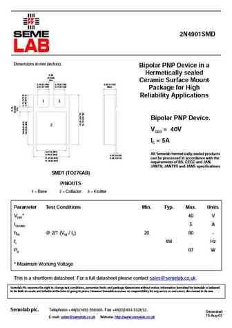
2N4901SMD Dimensions in mm (inches). Bipolar PNP Device in a Hermetically sealed 0.89 (0.035) min. Ceramic Surface Mount 3.70 (0.146) 3.70 (0.146) 3.60 (0.142) 3.41 (0.134) 3.41 (0.134) Max. Package for High Reliability Applications 1 3 Bipolar PNP Device. 2 VCEO = 40V IC = 5A 9.67 (0.381) All Semelab hermetically sealed products 9.38 (0.369) 0.50 (0.020) 0.26 (0
2n4910xsmd05.pdf
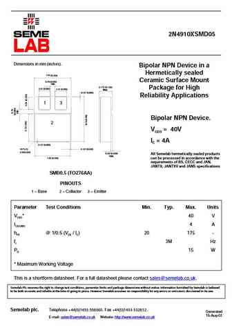
2N4910XSMD05 Dimensions in mm (inches). Bipolar NPN Device in a Hermetically sealed 7.54 (0.296) 0.76 (0.030) Ceramic Surface Mount min. 3.175 (0.125) 2.41 (0.095) Package for High 2.41 (0.095) Max. 0.127 (0.005) Reliability Applications 1 3 Bipolar NPN Device. 2 VCEO = 40V IC = 4A 0.127 (0.005) 16 PLCS 0.127 (0.005) 0.50(0.020) 0.50 (0.020) All Semelab her
2n4925.pdf
2N4925 Dimensions in mm (inches). Bipolar NPN Device in a 8.51 (0.34) 9.40 (0.37) Hermetically sealed TO39 7.75 (0.305) 8.51 (0.335) Metal Package. 6.10 (0.240) 6.60 (0.260) Bipolar NPN Device. 0.89 max. (0.035) 12.70 (0.500) min. 0.41 (0.016) 0.53 (0.021) VCEO = 150V dia. IC = 0.2A 5.08 (0.200) typ. 2.54 All Semelab hermetically sealed products 2 (0.100) 1
2n4911xsmd05.pdf
2N4911XSMD05 Dimensions in mm (inches). Bipolar NPN Device in a Hermetically sealed 7.54 (0.296) 0.76 (0.030) Ceramic Surface Mount min. 3.175 (0.125) 2.41 (0.095) Package for High 2.41 (0.095) Max. 0.127 (0.005) Reliability Applications 1 3 Bipolar NPN Device. 2 VCEO = 60V IC = 4A 0.127 (0.005) 16 PLCS 0.127 (0.005) 0.50(0.020) 0.50 (0.020) All Semelab her
2n4910x 2n4911x 2n4912x.pdf
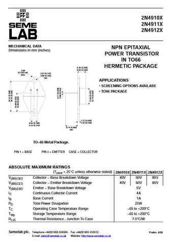
2N4910X 2N4911X 2N4912X MECHANICAL DATA NPN EPITAXIAL Dimensions in mm (inches) POWER TRANSISTOR IN TO66 HERMETIC PACKAGE 6.35 (0.250) 8.64 (0.340) 3.68 (0.145) rad. 3.61 (0.142) max. 3.86 (0.145) rad. APPLICATIONS SCREENING OPTIONS AVAILABE 1 2 TO66 PACKAGE 1.27 (0.050) 1.91 (0.750) 4.83 (0.190) 5.33 (0.210) 9.14 (0.360) min. TO 66 Metal Package. PIN 1 =
2n4928dcsm.pdf
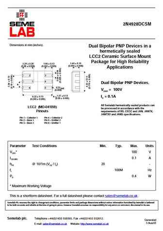
2N4928DCSM Dimensions in mm (inches). Dual Bipolar PNP Devices in a hermetically sealed LCC2 Ceramic Surface Mount Package for High Reliability 1.40 0.15 2.29 0.20 1.65 0.13 (0.055 0.006) (0.09 0.008) (0.065 0.005) Applications 2 3 1 4 Dual Bipolar PNP Devices. A 0.23 6 5 rad. (0.009) V = 100V CEO 6.22 0.13 A = 1.27 0.13 I = 0.1A C (0.
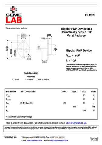
2n4909.pdf
2N4909 Dimensions in mm (inches). Bipolar PNP Device in a Hermetically sealed TO3 25.15 (0.99) 6.35 (0.25) 26.67 (1.05) 9.15 (0.36) Metal Package. 10.67 (0.42) 11.18 (0.44) 1.52 (0.06) 3.43 (0.135) 1 2 Bipolar PNP Device. 3 VCEO = 80V (case) 3.84 (0.151) 4.09 (0.161) 7.92 (0.312) IC = 10A 12.70 (0.50) All Semelab hermetically sealed products can be processed in a
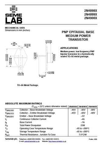
2n4900x.pdf
2N4898X 2N4899X 2N4900X MECHANICAL DATA Dimensions in mm (inches) PNP EPITAXIAL BASE MEDIUM POWER TRANSISTOR 6.35 (0.250) 8.64 (0.340) 3.68 (0.145) rad. 3.61 (0.142) max. 3.86 (0.145) rad. APPLICATIONS Medium power, low frequency PNP bipolar transistor in a hermetically sealed TO 66 metal package. 1.27 (0.050) 1.91 (0.750) 4.83 (0.190) 5.33 (0.210) 9.14 (0.360) min.
2n4910xsmd.pdf
2N4910XSMD Dimensions in mm (inches). Bipolar NPN Device in a Hermetically sealed 0.89 (0.035) min. Ceramic Surface Mount 3.70 (0.146) 3.70 (0.146) 3.60 (0.142) 3.41 (0.134) 3.41 (0.134) Max. Package for High Reliability Applications 1 3 Bipolar NPN Device. 2 VCEO = 40V IC = 4A 9.67 (0.381) All Semelab hermetically sealed products 9.38 (0.369) 0.50 (0.020) 0.26 (
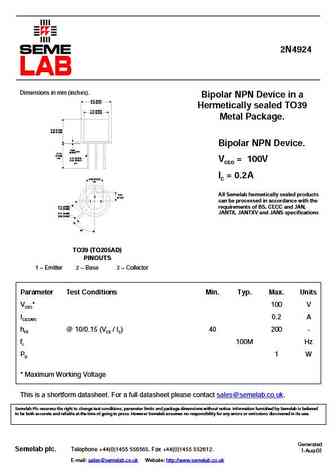
2n4924.pdf
2N4924 Dimensions in mm (inches). Bipolar NPN Device in a 8.51 (0.34) 9.40 (0.37) Hermetically sealed TO39 7.75 (0.305) 8.51 (0.335) Metal Package. 6.10 (0.240) 6.60 (0.260) Bipolar NPN Device. 0.89 max. (0.035) 12.70 (0.500) min. 0.41 (0.016) 0.53 (0.021) VCEO = 100V dia. IC = 0.2A 5.08 (0.200) typ. 2.54 All Semelab hermetically sealed products 2 (0.100) 1
2n4907.pdf
2N4907 Dimensions in mm (inches). Bipolar PNP Device in a Hermetically sealed TO3 25.15 (0.99) 6.35 (0.25) 26.67 (1.05) 9.15 (0.36) Metal Package. 10.67 (0.42) 11.18 (0.44) 1.52 (0.06) 3.43 (0.135) 1 2 Bipolar PNP Device. 3 VCEO = 40V (case) 3.84 (0.151) 4.09 (0.161) 7.92 (0.312) IC = 10A 12.70 (0.50) All Semelab hermetically sealed products can be processed in a
2n4911xsmd.pdf
2N4911XSMD Dimensions in mm (inches). Bipolar NPN Device in a Hermetically sealed 0.89 (0.035) min. Ceramic Surface Mount 3.70 (0.146) 3.70 (0.146) 3.60 (0.142) 3.41 (0.134) 3.41 (0.134) Max. Package for High Reliability Applications 1 3 Bipolar NPN Device. 2 VCEO = 60V IC = 4A 9.67 (0.381) All Semelab hermetically sealed products 9.38 (0.369) 0.50 (0.020) 0.26 (
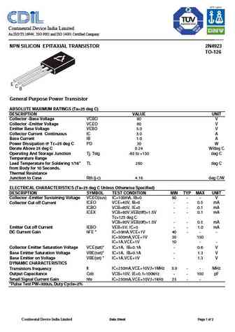
2n4923.pdf
Continental Device India Limited An ISO/TS 16949, ISO 9001 and ISO 14001 Certified Company NPN SILICON EPITAXIAL TRANSISTOR 2N4923 TO-126 E C B General Purpose Power Transistor ABSOLUTE MAXIMUM RATINGS (Ta=25 deg C) DESCRIPTION VALUE UNIT Collector -Base Voltage VCBO 80 V Collector -Emitter Voltage VCEO 80 V Emitter Base Voltage VEBO 5.0 V Collector Current Continuous IC 3.0 A Bas
2n4918 2n4919 2n4920.pdf
Product Specification www.jmnic.com Silicon PNP Power Transistors 2N4918 2N4919 2N4920 DESCRIPTION With TO-126 package Complement to type 2N4921,2N4922 2N4923 Excellent safe operating area Low collector-emitter saturation voltage APPLICATIONS For driver circuits ,switching ,and amplifier applications PINNING PIN DESCRIPTION 1 Emitter Collector;connected to
2n4921 2n4922 2n4923.pdf
Product Specification www.jmnic.com Silicon NPN Power Transistors 2N4921 2N4922 2N4923 DESCRIPTION With TO-126 package Complement to type 2N4918,2N4919 2N4920 Excellent safe operating area Low collector-emitter saturation voltage APPLICATIONS For driver circuits ,switching ,and amplifier applications PINNING PIN DESCRIPTION 1 Emitter Collector;connected to
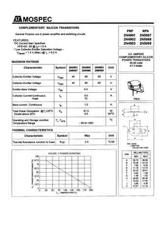
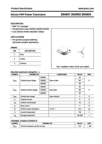
2n4901 2n4902 2n4903.pdf
Product Specification www.jmnic.com Silicon PNP Power Transistors 2N4901 2N4902 2N4903 DESCRIPTION With TO-3 package Complement to type 2N5067,2N5068,2N5069 Low collector-emitter saturation voltage APPLICATIONS For general purpose switching and power amplifier applications. PINNING PIN DESCRIPTION 1 Base 2 Emitter 3 Collector Fig.1 simplified outline (TO-3) an
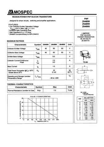
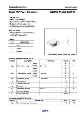
2n4898 2n4899 2n4900.pdf
Product Specification www.jmnic.com Silicon PNP Power Transistors 2N4898 2N4899 2N4900 DESCRIPTION With TO-66 package Low collector-emitter saturation voltage Excellent safe operating area 2N4900 complement to type 2N4912 APPLICATIONS Designed for driver circuits,switching and amplifier applications PINNING PIN DESCRIPTION 1 Base 2 Emitter 3 Collector Fi
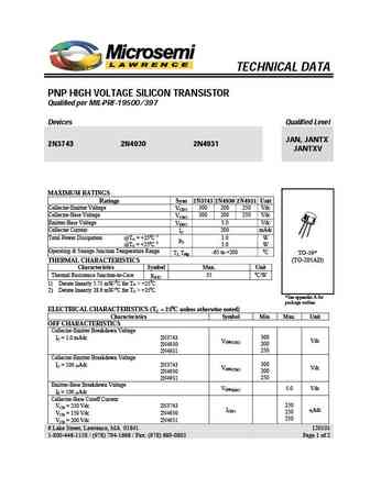
2n3743 2n4930 2n4931.pdf
TECHNICAL DATA PNP HIGH VOLTAGE SILICON TRANSISTOR Qualified per MIL-PRF-19500/397 Devices Qualified Level JAN, JANTX 2N3743 2N4930 2N4931 JANTXV MAXIMUM RATINGS Ratings Sym 2N3743 2N4930 2N4931 Unit Collector-Emitter Voltage 300 200 250 Vdc VCEO Collector-Base Voltage 300 200 250 Vdc VCBO Emitter-Base Voltage 5.0 Vdc VEBO Collector Current 200 mAdc IC Total
2n4991.pdf
2N4991 Silicon bilateral switch (SBS) in package TO-92 0.45max 0.7max 1 5.2 2.5 2 14.5 1.6 5.2 3 4.2 Pinouts 1- Anode II, 2- Gate, 3- Anode I Ratings Symbol Parameter, units Limits IT(rms) DC forward anode current, mA 200 Igm DC gate current, mA 5 IT(sm) Peak recurrent forward current, A, (1% duty cycle, 10 sec pulse width) 1 P Power dissipation, mW 300
2n4992.pdf
2N4992 Silicon bilateral switch (SBS) in package TO-92 0.45max 0.7max 1 5.2 2.5 2 14.5 1.6 5.2 3 4.2 Pinouts 1- Anode II, 2- Gate, 3- Anode I Ratings Symbol Parameter, units Limits IT(rms) DC forward anode current, mA 200 Igm DC gate current, mA 5 IT(sm) Peak recurrent forward current, A, (1% duty cycle, 10 sec pulse width) 1 P Power dissipation, mW 300 Electri
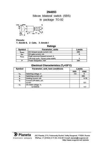
2n4993.pdf
2N4993 Silicon bilateral switch (SBS) in package TO-92 0.45max 0.7max 1 5.2 2.5 2 14.5 1.6 5.2 3 4.2 Pinouts 1- Anode II, 2- Gate, 3- Anode I Ratings Symbol Parameter, units Limits IT(rms) DC forward anode current, mA 200 Igm DC gate current, mA 5 IT(sm) Peak recurrent forward current, A, (1% duty cycle, 10 sec pulse width) 1 P Power dissipation, mW 300
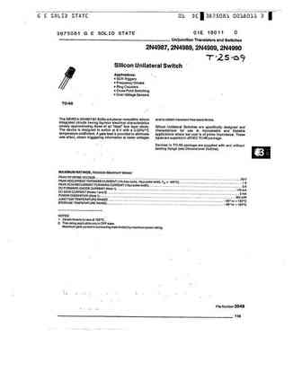
2n4987.pdf
2N4987 Silicon unilateral switch (SUS) in package TO-92 0.45max 0.7max 1 5.2 2.5 2 14.5 1.6 5.2 3 4.2 Pinouts 1- Cathode, 2- Gate, 3- Anode Ratings Symbol Parameter, units Limits Vrrm Peak reverse voltage, V -30 IT(rms) DC forward anode current, mA 175 Igm DC gate current, mA 5 IT(sm) Peak recurrent forward current, A, (1% duty cycle, 10 sec pulse width)
2n4988.pdf
2N4988 Silicon unilateral switch (SUS) in package TO-92 0.45max 0.7max 1 5.2 2.5 2 14.5 1.6 5.2 3 4.2 Pinouts 1- Cathode, 2- Gate, 3- Anode Ratings Symbol Parameter, units Limits Vrrm Peak reverse voltage, V -30 IT(rms) DC forward anode current, mA 175 Igm DC gate current, mA 5 IT(sm) Peak recurrent forward current, A, (1% duty cycle, 10 sec pulse width)
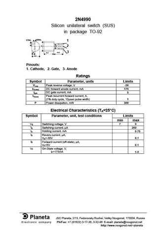
2n4990.pdf
2N4990 Silicon unilateral switch (SUS) in package TO-92 0.45max 0.7max 1 5.2 2.5 2 14.5 1.6 5.2 3 4.2 Pinouts 1- Cathode, 2- Gate, 3- Anode Ratings Symbol Parameter, units Limits Vrrm Peak reverse voltage, V -30 IT(rms) DC forward anode current, mA 175 Igm DC gate current, mA 5 IT(sm) Peak recurrent forward current, A, (1% duty cycle, 10 sec pulse width)
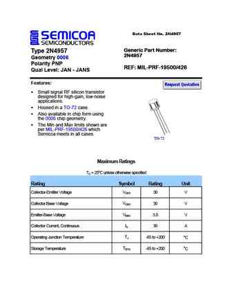
2n4957.pdf
Data Sheet No. 2N4957 Generic Part Number Type 2N4957 2N4957 Geometry 0006 Polarity PNP REF MIL-PRF-19500/426 Qual Level JAN - JANS Features Small signal RF silicon transistor designed for high-gain, low-noise applications. Housed in a TO-72 case. Also available in chip form using the 0006 chip geometry. The Min and Max limits shown are per MIL-PRF-19500/426
2n4265 2n4400 2n4401 2n4402 2n4403 2n4409 2n4410 2n4424 2n4425 2n4951 2n4952 2n4953 2n4954 2n5087 2n5088 2n5089.pdf
2n4922.pdf
INCHANGE Semiconductor isc Silicon NPN Power Transistor 2N4922 DESCRIPTION Collector-Emitter Sustaining Voltage- V = 60V(Min) CEO(SUS) Low Collector Saturatioin Voltage- V = 0.6V(Max.)@ I = 1A CE(sat) C Wide Area of Safe Operation Complement to Type 2N4919 Minimum Lot-to-Lot variations for robust device performance and reliable operation APPLICATIONS Designed for d
2n4918 2n4919 2n4920.pdf
Inchange Semiconductor Product Specification Silicon PNP Power Transistors 2N4918 2N4919 2N4920 DESCRIPTION With TO-126 package Complement to type 2N4921/4922/4923 Excellent safe operating area Low collector saturation voltage APPLICATIONS For driver circuits ,switching ,and amplifier applications PINNING PIN DESCRIPTION 1 Emitter Collector;connected to 2
2n4915.pdf
INCHANGE Semiconductor isc Product Specification isc Silicon NPN Power Transistors 2N4915 DESCRIPTION Low Collector Saturation Voltage- VCE(sat)= 1.5V(Max.)@ IC= 5A DC Current Gain- hFE= 25-100 @IC= 2.5A Complement to Type 2N4906 APPLICATIONS Designed for general purpose use in power amplifier and switching circuits. ABSOLUTE MAXIMUM RATINGS(Ta=25 ) SYMB
2n4912.pdf
INCHANGE Semiconductor isc Product Specification isc Silicon NPN Power Transistor 2N4912 DESCRIPTION Collector-Emitter Sustaining Voltage- VCEO(SUS)= 80V(Min) Low Collector Saturatioin Voltage- VCE(sat)= 0.6V(Max.)@ IC= 1A Wide Area of Safe Operation Complement to Type 2N4900 APPLICATIONS Designed for driver circuits, switching and amplifier applications.
2n4918.pdf
INCHANGE Semiconductor isc Product Specification isc Silicon PNP Power Transistor 2N4918 DESCRIPTION Collector-Emitter Sustaining Voltage- VCEO(SUS)= -40V(Min) Low Collector Saturatioin Voltage- VCE(sat)= -0.6V(Max.)@ IC= -1A Wide Area of Safe Operation Complement to Type 2N4921 APPLICATIONS Designed for driver circuits, switching and amplifier application
2n4908.pdf
INCHANGE Semiconductor isc Product Specification isc Silicon PNP Power Transistors 2N4908 DESCRIPTION Low Collector Saturation Voltage- VCE(sat)= -0.75V(Max.)@ IC= -4A DC Current Gain- hFE= 20-80 @IC= -4A APPLICATIONS Designed for general purpose use in power amplifier and switching circuits. ABSOLUTE MAXIMUM RATINGS(Ta=25 ) SYMBOL PARAMETER VALUE UNIT VCB
2n4904 2n4905 2n4906.pdf
Inchange Semiconductor Product Specification Silicon PNP Power Transistors 2N4904 2N4905 2N4906 DESCRIPTION With TO-3 package Complement to type 2N4913/4914/4915 Low collector saturation voltage APPLICATIONS For general purpose switching and power amplifier applications. PINNING PIN DESCRIPTION 1 Base 2 Emitter Fig.1 simplified outline (TO-3) and symbol 3 Coll
2n4910.pdf
INCHANGE Semiconductor isc Product Specification isc Silicon NPN Power Transistor 2N4910 DESCRIPTION Collector-Emitter Sustaining Voltage- VCEO(SUS)= 40V(Min) Low Collector Saturatioin Voltage- VCE(sat)= 0.6V(Max.)@ IC= 1A Wide Area of Safe Operation APPLICATIONS Designed for driver circuits, switching and amplifier applications. ABSOLUTE MAXIMUM RATINGS(Ta=
2n4902.pdf
INCHANGE Semiconductor isc Product Specification isc Silicon PNP Power Transistors 2N4902 DESCRIPTION Low Collector Saturation Voltage- VCE(sat)= -1.5V(Max.)@ IC= -5A DC Current Gain- hFE= 20-80 @IC= -1A Complement to Type 2N5068 APPLICATIONS Designed for general purpose use in power amplifier and switching circuits. ABSOLUTE MAXIMUM RATINGS(Ta=25 ) SYMB
2n4914.pdf
INCHANGE Semiconductor isc Product Specification isc Silicon NPN Power Transistors 2N4914 DESCRIPTION Low Collector Saturation Voltage- VCE(sat)= 1.5V(Max.)@ IC= 5A DC Current Gain- hFE= 25-100 @IC= 2.5A Complement to Type 2N4905 APPLICATIONS Designed for general purpose use in power amplifier and switching circuits. ABSOLUTE MAXIMUM RATINGS(Ta=25 ) SYMB
2n4913.pdf
INCHANGE Semiconductor isc Product Specification isc Silicon NPN Power Transistors 2N4913 DESCRIPTION Low Collector Saturation Voltage- VCE(sat)= 1.5V(Max.)@ IC= 5A DC Current Gain- hFE= 25-100 @IC= 2.5A Complement to Type 2N4904 APPLICATIONS Designed for general purpose use in power amplifier and switching circuits. ABSOLUTE MAXIMUM RATINGS(Ta=25 ) SYMB
2n4921 2n4922 2n4923.pdf
Inchange Semiconductor Product Specification Silicon NPN Power Transistors 2N4921 2N4922 2N4923 DESCRIPTION With TO-126 package Complement to type 2N4918/4919/4920 Excellent safe operating area Low collector saturation voltage APPLICATIONS For driver circuits ,switching ,and amplifier applications PINNING PIN DESCRIPTION 1 Emitter Collector;connected to 2
2n4909.pdf
INCHANGE Semiconductor isc Product Specification isc Silicon PNP Power Transistors 2N4909 DESCRIPTION Low Collector Saturation Voltage- VCE(sat)= -0.75V(Max.)@ IC= -4A DC Current Gain- hFE= 20-80 @IC= -4A APPLICATIONS Designed for general purpose use in power amplifier and switching circuits. ABSOLUTE MAXIMUM RATINGS(Ta=25 ) SYMBOL PARAMETER VALUE UNIT VCB
2n4923.pdf
isc Silicon NPN Power Transistor 2N4923 DESCRIPTION Collector-Emitter Sustaining Voltage- V = 80V(Min) CEO(SUS) Low Collector Saturation Voltage- V = 0.6V(Max.)@ I = 1A CE(sat) C Wide Area of Safe Operation Complement to Type 2N4920 Minimum Lot-to-Lot variations for robust device performance and reliable operation APPLICATIONS Designed for driver circuits, switching
2n4903.pdf
INCHANGE Semiconductor isc Product Specification isc Silicon PNP Power Transistors 2N4903 DESCRIPTION Low Collector Saturation Voltage- VCE(sat)= -1.5V(Max.)@ IC= -5A DC Current Gain- hFE= 20-80 @IC= -1A Complement to Type 2N5069 APPLICATIONS Designed for general purpose use in power amplifier and switching circuits. ABSOLUTE MAXIMUM RATINGS(Ta=25 ) SYMB
2n4906.pdf
INCHANGE Semiconductor isc Product Specification isc Silicon PNP Power Transistors 2N4906 DESCRIPTION Low Collector Saturation Voltage- VCE(sat)= -1.5V(Max.)@ IC= -5A DC Current Gain- hFE= 25-100 @IC= -2.5A Complement to Type 2N4915 APPLICATIONS Designed for general purpose use in power amplifier and switching circuits. ABSOLUTE MAXIMUM RATINGS(Ta=25 ) S
2n4901 2n4902 2n4903.pdf
Inchange Semiconductor Product Specification Silicon PNP Power Transistors 2N4901 2N4902 2N4903 DESCRIPTION With TO-3 package Complement to type 2N5067/5068/5069 Low collector saturation voltage APPLICATIONS For general purpose switching and power amplifier applications. PINNING PIN DESCRIPTION 1 Base 2 Emitter Fig.1 simplified outline (TO-3) and symbol 3 Coll
2n4904.pdf
INCHANGE Semiconductor isc Product Specification isc Silicon PNP Power Transistors 2N4904 DESCRIPTION Low Collector Saturation Voltage- VCE(sat)= -1.5V(Max.)@ IC= -5A DC Current Gain- hFE= 25-100 @IC= -2.5A Complement to Type 2N4913 APPLICATIONS Designed for general purpose use in power amplifier and switching circuits. ABSOLUTE MAXIMUM RATINGS(Ta=25 ) S
2n4907.pdf
INCHANGE Semiconductor isc Product Specification isc Silicon PNP Power Transistors 2N4907 DESCRIPTION Low Collector Saturation Voltage- VCE(sat)= -0.75V(Max.)@ IC= -4A DC Current Gain- hFE= 20-80 @IC= -4A APPLICATIONS Designed for general purpose use in power amplifier and switching circuits. ABSOLUTE MAXIMUM RATINGS(Ta=25 ) SYMBOL PARAMETER VALUE UNIT VCB
2n4898 2n4899 2n4900.pdf
Inchange Semiconductor Product Specification Silicon PNP Power Transistors 2N4898 2N4899 2N4900 DESCRIPTION With TO-66 package Low collector saturation voltage Excellent safe operating area 2N4900 complement to type 2N4912 APPLICATIONS Designed for driver circuits,switching and amplifier applications PINNING PIN DESCRIPTION 1 Base 2 Emitter Fig.1 simplifi
2n4911.pdf
INCHANGE Semiconductor isc Product Specification isc Silicon NPN Power Transistor 2N4911 DESCRIPTION Collector-Emitter Sustaining Voltage- VCEO(SUS)= 60V(Min) Low Collector Saturatioin Voltage- VCE(sat)= 0.6V(Max.)@ IC= 1A Wide Area of Safe Operation APPLICATIONS Designed for driver circuits, switching and amplifier applications. ABSOLUTE MAXIMUM RATINGS(Ta=
Otros transistores... 2N4889, 2N4890, 2N4890S, 2N4895, 2N4896, 2N4897, 2N4898, 2N4899, BC639, 2N4900, 2N4901, 2N4901SM, 2N4902, 2N4903, 2N4904, 2N4905, 2N4906
Parámetros del transistor bipolar y su interrelación.
🌐 : EN ES РУ
Liste
Recientemente añadidas las descripciónes de los transistores:
BJT: ZDT6705 | GA1L4Z | GA1A4M | SBT42 | 2SA200-Y | 2SA200-O | 2SD882-Q | 2SD882-P | 2SD882-E | 2SC945-L | 2SC945-H | 2SC4226-R23 | 2SC3357-F | 2SC3357-E | 2SC3356-R26 | 2SC3356-R24 | 2SC3356-R23 | 2SB772-Q | 2SB772-P | 2SB772-E | 2SA1015-L
Popular searches
2n2923 | 2n2102 | mj15003g | oc75 transistor | irfp260m | 2sc1213 | a1491 transistor | 2sc897
