P401 Equivalente. Reemplazo. Hoja de especificaciones. Principales características
Número de Parte: P401
Material: Ge
Polaridad de transistor: PNP
ESPECIFICACIONES MÁXIMAS
Disipación total del dispositivo (Pc): 0.1 W
Tensión colector-base (Vcb): 10 V
Tensión colector-emisor (Vce): 10 V
Tensión emisor-base (Veb): 1 V
Corriente del colector DC máxima (Ic): 0.02 A
Temperatura operativa máxima (Tj): 75 °C
CARACTERÍSTICAS ELÉCTRICAS
Transición de frecuencia (fT): 30 MHz
Capacitancia de salida (Cc): 15 pF
Ganancia de corriente contínua (hFE): 16
Búsqueda de reemplazo de P401
- Selecciónⓘ de transistores por parámetros
P401 datasheet
0.1. Size:359K 1
dmp4015sps-13.pdf 
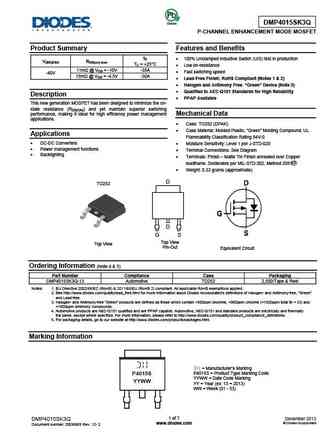
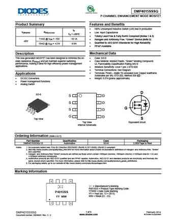
DMP4015SPS Green 40V P-CHANNEL ENHANCEMENT MODE MOSFET POWERDI Product Summary Features and Benefits 100% Unclamped Inductive Switch (UIS) Test In Production ID V(BR)DSS RDS(on) max TA = +25 C Low On-Resistance Fast Switching Speed 11m @ VGS = -10V -17A -40V Lead-Free Finish; RoHS Compliant (Notes 1 & 2) 15m @ VGS = -4.5V -14.5A Halogen and
0.2. Size:177K toshiba
mp4015 .pdf
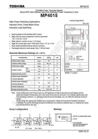
MP4015 TOSHIBA Power Transistor Module Silicon NPN Triple Diffused Type (Four Darlington Power Transistors in One) MP4015 Industrial Applications High Power Switching Applications Unit mm Hammer Drive, Pulse Motor Drive Inductive Load Switching Small package by full molding (SIP 10 pins) High collector power dissipation (4-device operation) PT = 4 W (Ta = 25 C)
0.3. Size:130K toshiba
mp4015.pdf
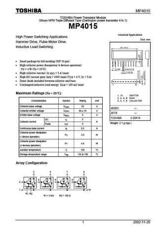
MP4015 TOSHIBA Power Transistor Module Silicon NPN Triple Diffused Type (Darlington power transistor 4 in 1) MP4015 Industrial Applications High Power Switching Applications. Unit mm Hammer Drive, Pulse Motor Drive. Inductive Load Switching. Small package by full molding (SIP 10 pin) High collector power dissipation (4 devices operation) P = 4 W (Ta = 25 C) T
0.4. Size:126K toshiba
mp4013.pdf
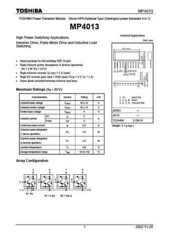
MP4013 TOSHIBA Power Transistor Module Silicon NPN Epitaxial Type (Darlington power transistor 4 in 1) MP4013 Industrial Applications High Power Switching Applications. Unit mm Hammer Drive, Pulse Motor Drive and Inductive Load Switching. Small package by full molding (SIP 10 pin) High collector power dissipation (4 devices operation) P = 4 W (Ta = 25 C) T
0.5. Size:167K toshiba
mp4013 .pdf
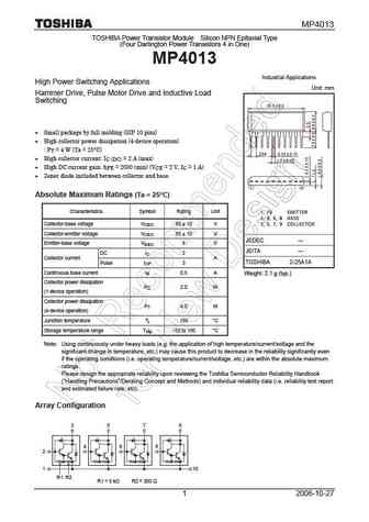
MP4013 TOSHIBA Power Transistor Module Silicon NPN Epitaxial Type (Four Darlington Power Transistors 4 in One) MP4013 Industrial Applications High Power Switching Applications Unit mm Hammer Drive, Pulse Motor Drive and Inductive Load Switching Small package by full molding (SIP 10 pins) High collector power dissipation (4-device operation) PT = 4 W (Ta = 25 C)
0.6. Size:92K sanyo
fp401.pdf
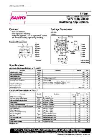
Ordering number EN4632 FP401 N-Channel MOS Silicon FET Very High-Speed Switching Applications Features Package Dimensions Low ON resistance. unit mm Very high-speed switching. 2102A Composite type with 2 low-voltage-drive N-channel [FP401] MOSFETs facilitating high-density mounting. Electrical Connection 1 Gate 1 Gate 2 Drain 2 Drain 3 Source 3 Source 4 Drain 4
0.7. Size:79K renesas
rjp4010age.pdf
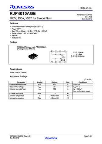
Preliminary Datasheet RJP4010AGE R07DS0371EJ0400 Rev.4.00 400V, 150A, IGBT for Strobe Flash Dec 28, 2012 Features Ultra small surface mount package (TSOJ-8) VCES 400 V ICM 150 A @VGE = 3 V, Tc = 70 C, CM = 100 F Drive voltage 3.0 V to 6 V (MAX) Pb-free Halogen-free Outline RENESAS Package code PTSJ0008JA-A (Package name TSOJ-8) 8 7 6
0.8. Size:148K siemens
bup401.pdf
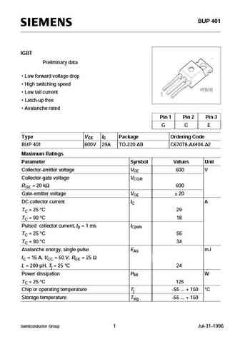
BUP 401 IGBT Preliminary data Low forward voltage drop High switching speed Low tail current Latch-up free Avalanche rated Pin 1 Pin 2 Pin 3 G C E Type VCE IC Package Ordering Code BUP 401 600V 29A TO-220 AB C67078-A4404-A2 Maximum Ratings Parameter Symbol Values Unit Collector-emitter voltage VCE 600 V Collector-gate voltage VCGR RGE = 20 k 600 Gate-emi
0.9. Size:363K diodes
dmp4015spsq.pdf
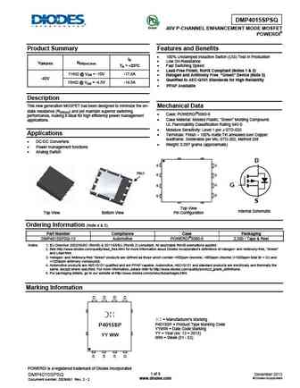
DMP4015SPSQ Green 40V P-CHANNEL ENHANCEMENT MODE MOSFET POWERDI Product Summary Features and Benefits 100% Unclamped Inductive Switch (UIS) Test In Production ID Low On-Resistance V(BR)DSS RDS(on) max TA = +25 C Fast Switching Speed Lead-Free Finish; RoHS Compliant (Notes 1 & 2) 11m @ VGS = -10V -17.0A Halogen and Antimony Free. Green Device
0.10. Size:270K diodes
dmp4015sssq.pdf
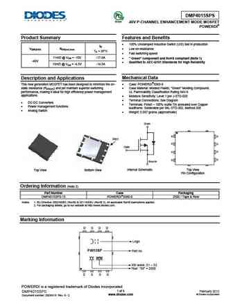
DMP4015SSSQ P-CHANNEL ENHANCEMENT MODE MOSFET Product Summary Features and Benefits 100% Unclamped Inductive Switch (UIS) test in production ID V(BR)DSS RDS(on) max Low Input Capacitance TA = +25 C Totally Lead-Free & Fully RoHS Compliant (Notes 1 & 2) 11m @ VGS = -10V -10.1A Halogen and Antimony Free. Green Device (Note 3) -40V Qualified to
0.11. Size:202K diodes
dmp4015sps.pdf
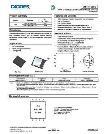
DMP4015SPS Green 40V P-CHANNEL ENHANCEMENT MODE MOSFET POWERDI Product Summary Features and Benefits 100% Unclamped Inductive Switch (UIS) test in production ID V(BR)DSS RDS(on) max Low on-resistance TA = 25 C Fast switching speed 11m @ VGS = -10V -17.0A " Green component and RoHS compliant (Note 1) -40V Qualified to AEC-Q101 Standards for Hig
0.12. Size:224K diodes
dmp4015sk3.pdf
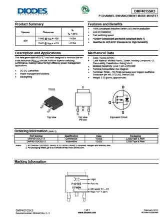
DMP4015SK3 P-CHANNEL ENHANCEMENT MODE MOSFET Product Summary Features and Benefits 100% Unclamped Inductive Switch (UIS) test in production ID V(BR)DSS RDS(on) max Low on-resistance TA = 25 C Fast switching speed 11m @ VGS = -10V -14.0A Green component and RoHS compliant (Note 1) -40V Qualified to AEC-Q101 Standards for High Reliability 15m
0.14. Size:516K diodes
dmp4013lfg.pdf
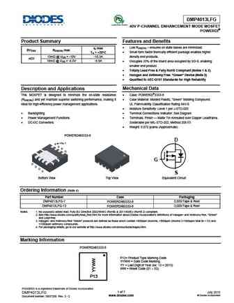
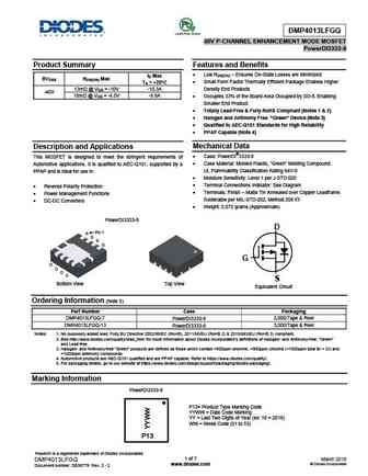
DMP4013LFG 40V P-CHANNEL ENHANCEMENT MODE MOSFET POWERDI Product Summary Features and Benefits Low RDS(ON) ensures on state losses are minimized. ID max BVDSS RDS(ON) max Small form factor thermally efficient package enables higher TA = +25 C 13m @ VGS = -10V -10.3A density end products. -40V 18m @ VGS = -4.5V -8.8A Occupies 33% of the board area
0.15. Size:603K diodes
dmp4013lfgq.pdf
DMP4013LFGQ 40V P-CHANNEL ENHANCEMENT MODE MOSFET PowerDI3333-8 Product Summary Features and Benefits Low RDS(ON) Ensures On-State Losses are Minimized ID Max BVDSS RDS(ON) Max Small Form Factor Thermally Efficient Package Enables Higher TA = +25 C 13m @ VGS = -10V -10.3A Density End Products -40V 18m @ VGS = -4.5V -8.8A Occupies 33% of the Board
0.16. Size:189K diodes
dmp4015sss.pdf
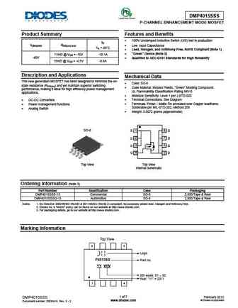
DMP4015SSS P-CHANNEL ENHANCEMENT MODE MOSFET Product Summary Features and Benefits 100% Unclamped Inductive Switch (UIS) test in production ID V(BR)DSS RDS(on) max Low Input Capacitance TA = 25 C Lead, Halogen, and Antimony Free, RoHS Compliant (Note 1) "Green" Device (Note 2) 11m @ VGS = -10V -10.1A -40V Qualified to AEC-Q101 Standards for High Rel
0.17. Size:259K onsemi
atp401.pdf
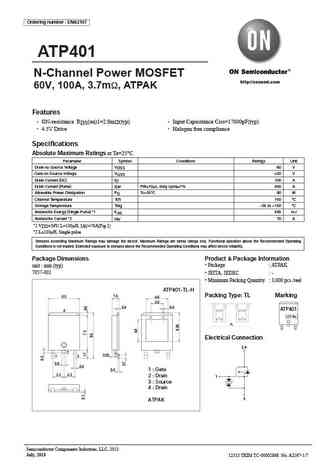
Ordering number ENA2167 ATP401 N-Channel Power MOSFET http //onsemi.com 60V, 100A, 3.7m , ATPAK Features ON-resistance RDS(on)1=2.8m (typ) Input Capasitance Ciss=17000pF(typ) 4.5V Drive Halogen free compliance Specifications Absolute Maximum Ratings at Ta=25 C Parameter Symbol Conditions Ratings Unit Drain-to-Source Voltage VDSS 60 V Gate-to-Source Vo
0.19. Size:1465K winsok
wsp4016.pdf
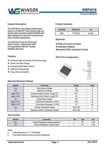
WSP4016 N-Channel MOSFET General Description Product Summery The WSP4016 is the highest performance BVDSS RDSON ID trench N-ch MOSFET with extreme high cell density,which provide excellent RDSON and 40V 11.5m 15.5A gate chargens for most of the synchronous buck converter applications . Applicatio The WSP4016 meet the RoHS and White LED boost converters Green Product r
0.20. Size:1482K cn vbsemi
dmp4015sssq.pdf
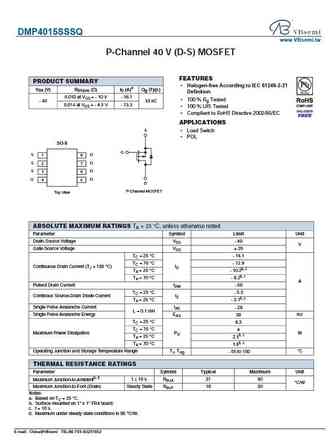
DMP4015SSSQ www.VBsemi.tw P-Channel 40 V (D-S) MOSFET FEATURES PRODUCT SUMMARY Halogen-free According to IEC 61249-2-21 VDS (V) RDS(on) ( )ID (A)a Qg (Typ.) Definition 0.010 at VGS = - 10 V - 16.1 100 % Rg Tested - 40 33 nC 0.014 at VGS = - 4.5 V - 13.3 100 % UIS Tested Compliant to RoHS Directive 2002/95/EC APPLICATIONS S Load Switch POL SO-8 G SD
0.21. Size:266K inchange semiconductor
dmp4015sk3.pdf
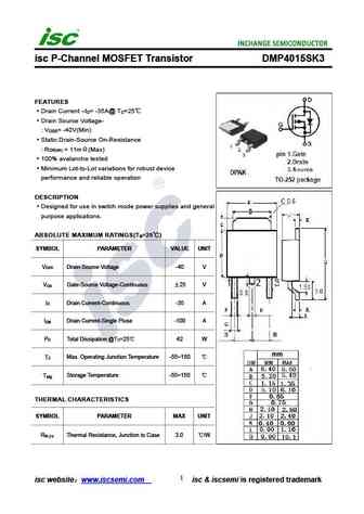
isc P-Channel MOSFET Transistor DMP4015SK3 FEATURES Drain Current I = -35A@ T =25 D C Drain Source Voltage- V = -40V(Min) DSS Static Drain-Source On-Resistance R = 11m (Max) DS(on) 100% avalanche tested Minimum Lot-to-Lot variations for robust device performance and reliable operation DESCRIPTION Designed for use in switch mode power supplies and general pu
Otros transistores... P306A, P307, P307A, P307B, P307G, P307V, P308, P309, BC547, P402, P403, P403A, P416, P416A, P416B, P417, P417A